Intel 正式推出代號 Alder Lake 的第 12 代 Core 桌上型處理器,採用 Intel 7 製程,導入混合式核心架構,佐以 Thread Director 技術帶來更優異的多核資源調度。首批推出 6 款 K 系列不鎖倍頻(KF 系列無內顯)產品,最高階 Core i9-12900K 定價 US$ 589,11 月 4 日開賣。
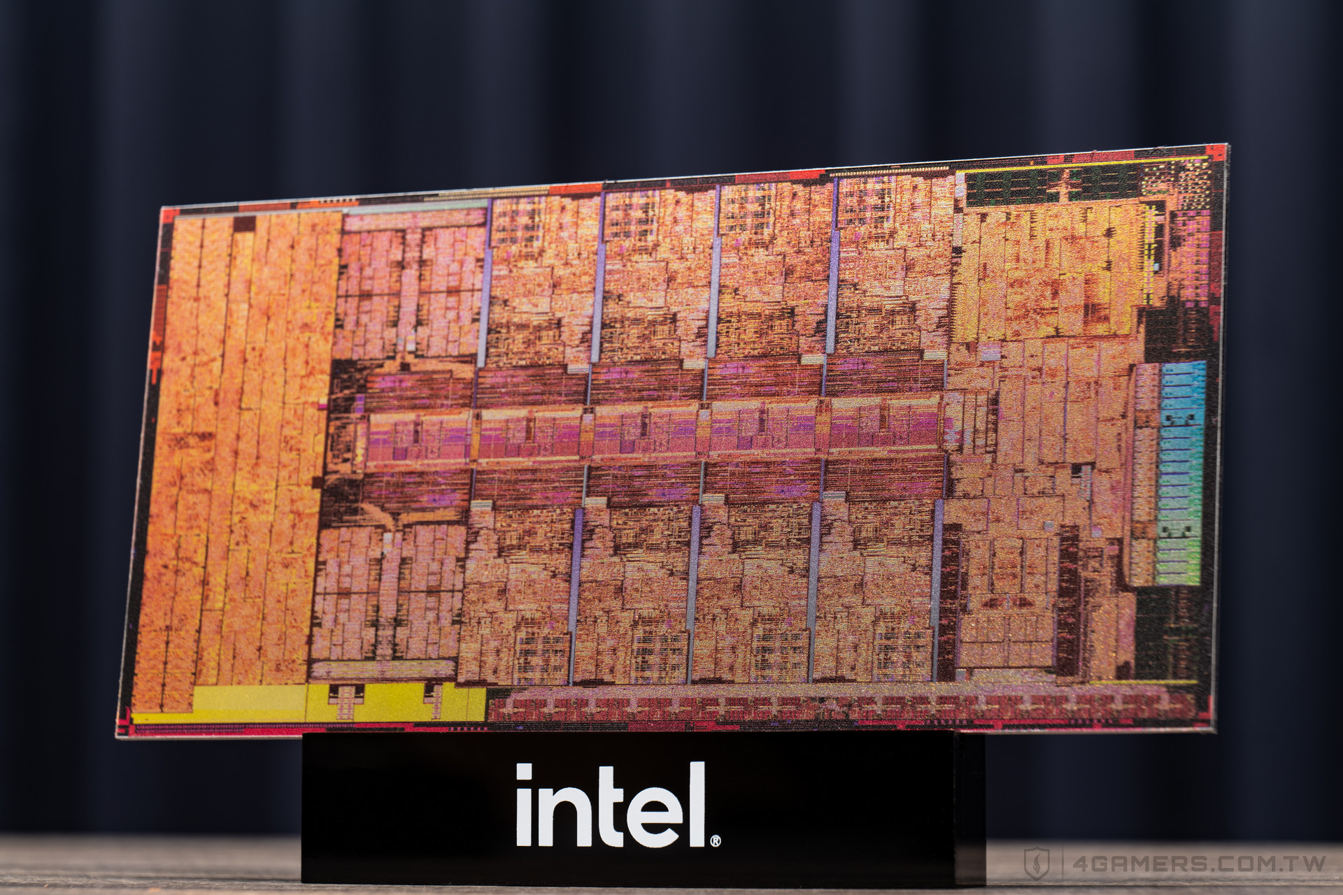
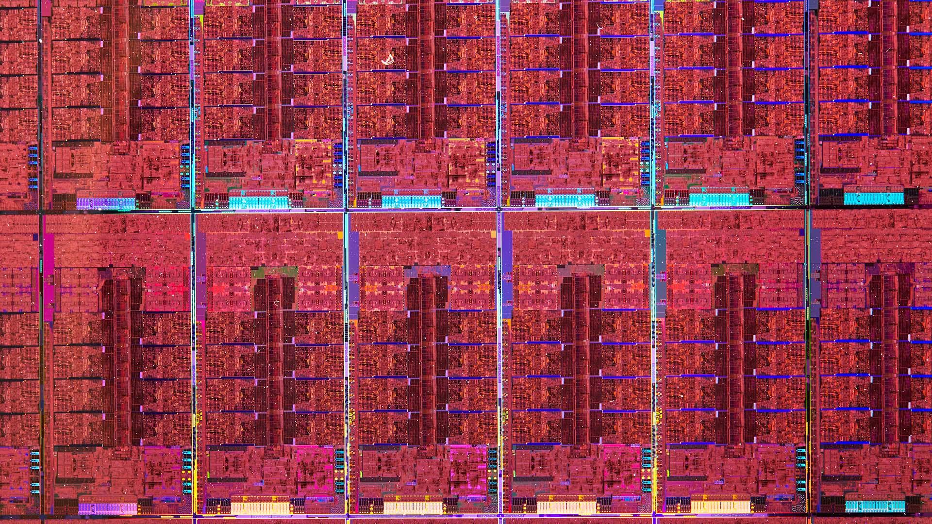 Alder Lake 晶圓照
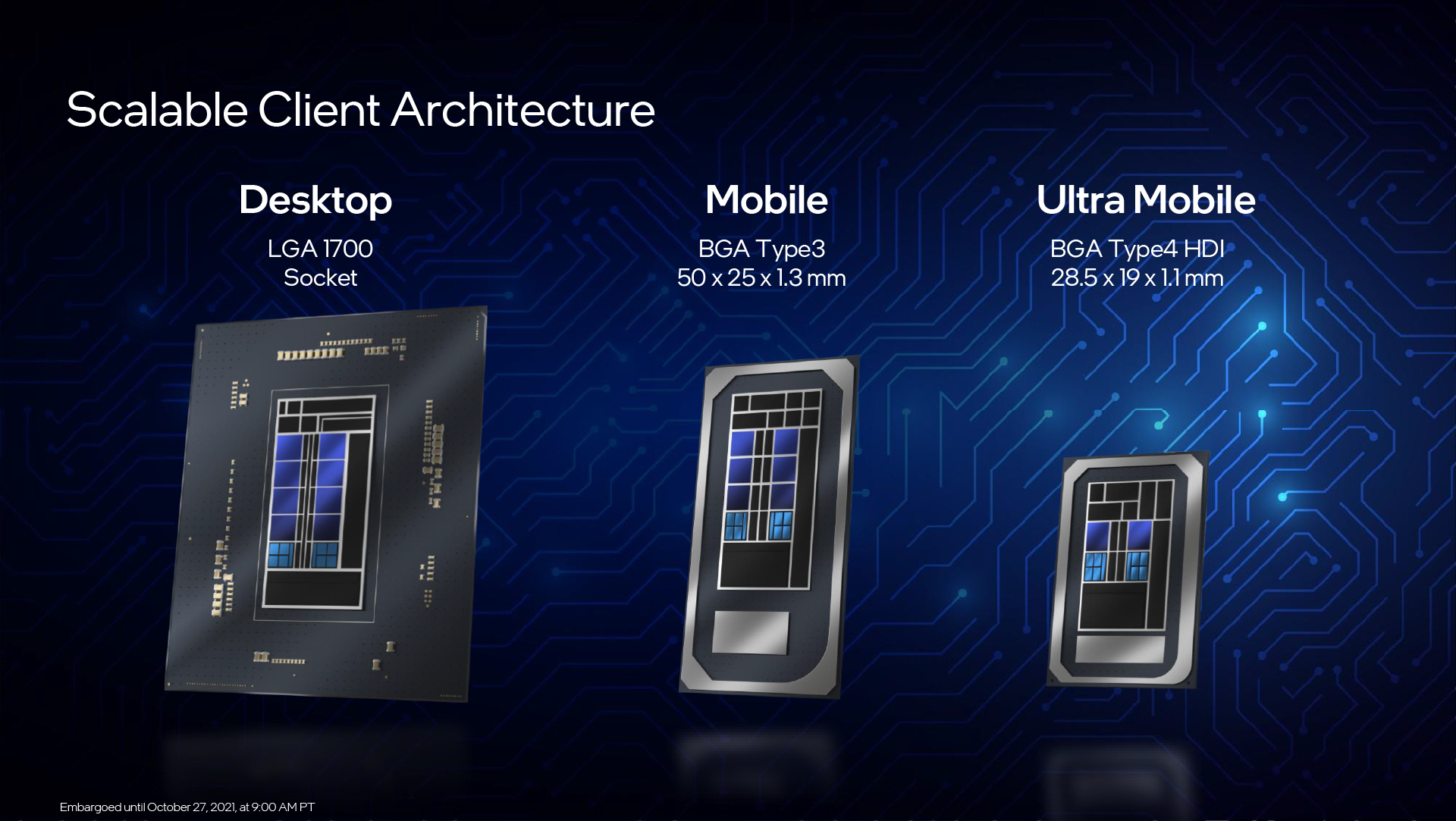
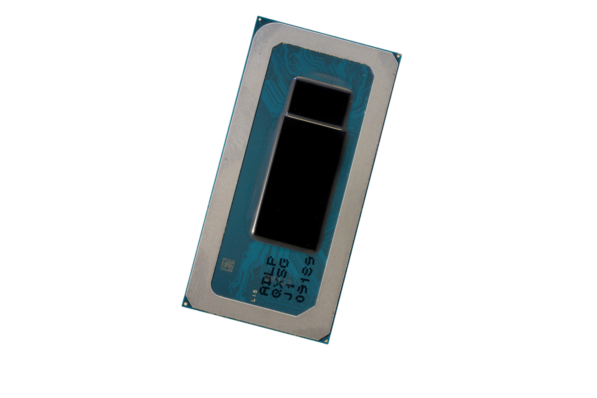 筆電版 Alder Lake 封裝
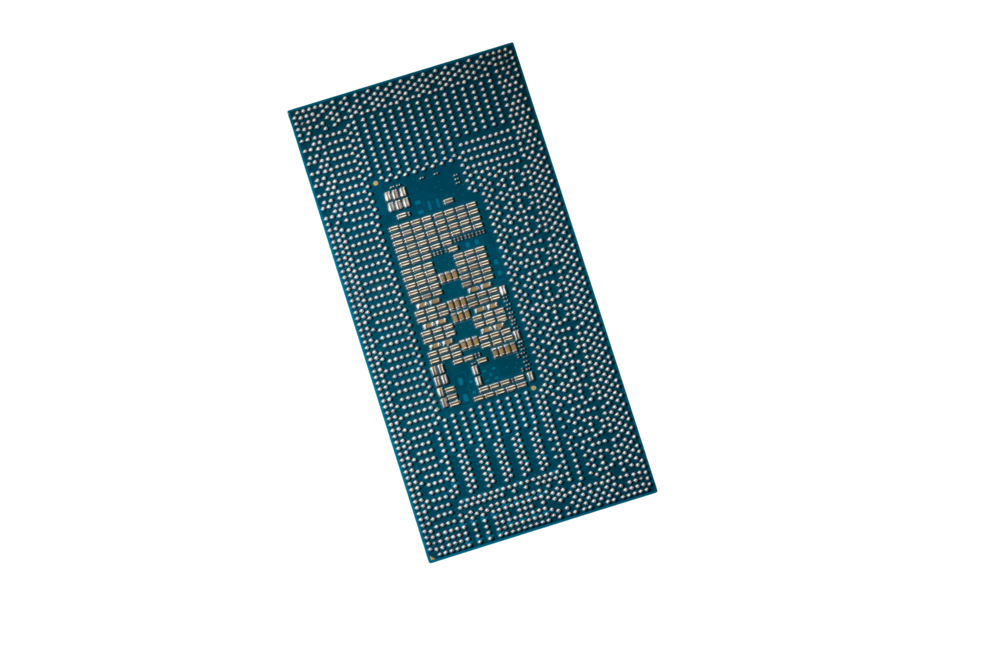 筆電版 Alder Lake 封裝
Intel Alder Lake 第 12 代 Core 桌上型 CPU 正式規格
| 產品 |
P-Core
數量 |
E-Core
數量 |
核心/執行緒
總數 |
P-Core
基礎/最高Boost時脈 |
E-Core
基礎/最高Boost時脈 |
L2 + L3 快取 |
處理器基礎功耗
(PL1 TDP) |
最大Turbo功耗
(PL2 TDP) |
定價
(千顆報價) |
| Core i9-12900K |
8 |
8 |
16 / 24 |
3.2 / 5.2 GHz |
2.4 / 3.9 GHz |
14 + 30 MB |
125W |
241W |
US$ 589 |
| Core i9-12900KF |
8 |
8 |
16 / 24 |
3.2 / 5.2 GHz |
2.4 / 3.9 GHz |
14 + 30 MB |
125W |
241W |
US$ 564 |
| Core i7-12700K |
8 |
4 |
12 / 20 |
3.6 / 5.0 GHz |
2.7 / 3.8 GHz |
12 + 25 MB |
125W |
190W |
US$ 409 |
| Core i7-12700KF |
8 |
4 |
12 / 20 |
3.6 / 5.0 GHz |
2.7 / 3.8 GHz |
12 + 25 MB |
125W |
190W |
US$ 384 |
| Core i5-12600K |
6 |
4 |
10 / 16 |
3.7 / 4.9 GHz |
2.8 / 3.6 GHz |
9.5 + 20 MB |
125W |
150W |
US$ 289 |
| Core i5-12600KF |
6 |
4 |
10 / 16 |
3.7 / 4.9 GHz |
2.8 / 3.6 GHz |
9.5 + 20 MB |
125W |
150W |
US$ 264 |
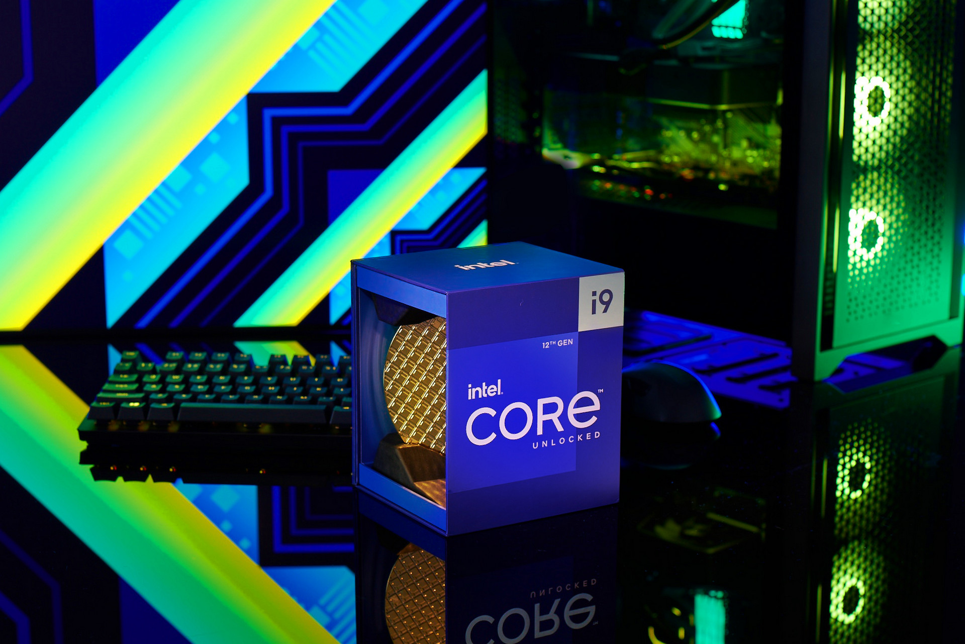
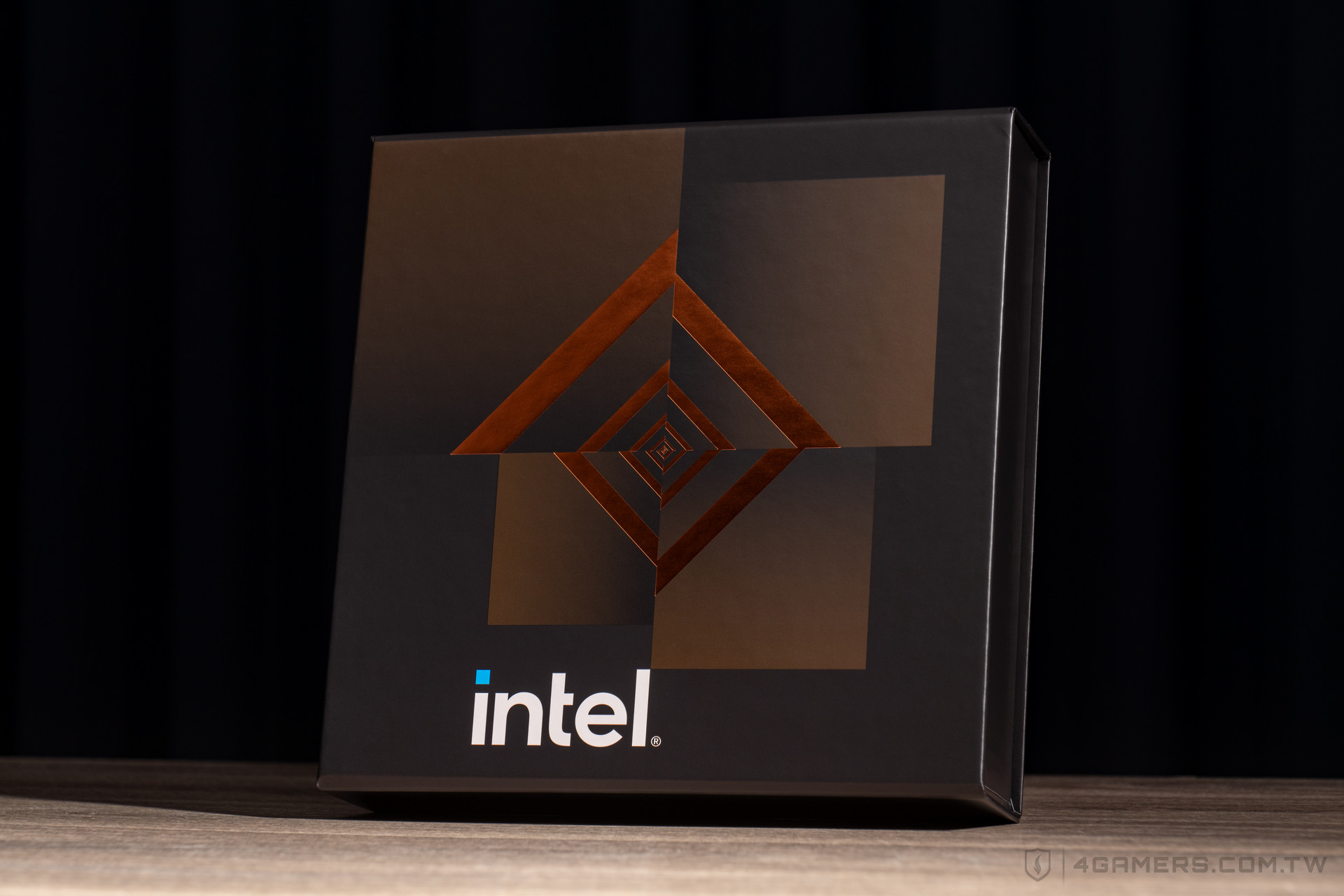
第 12 代 Intel Core 處理器媒體評測套裝
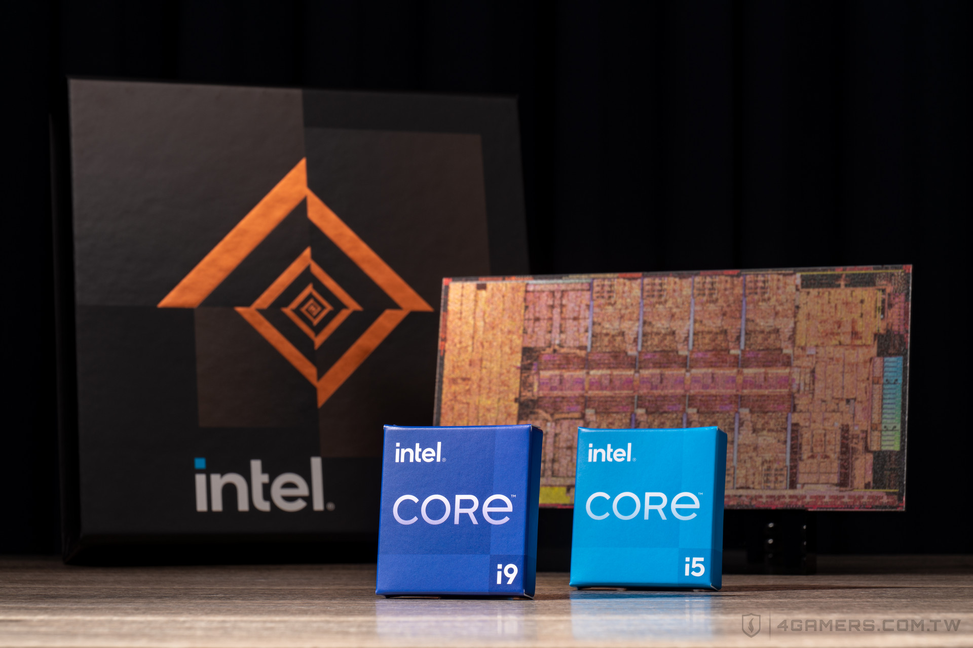
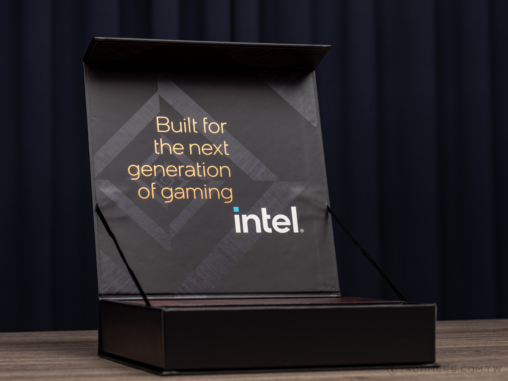
本次外盒視覺概念引入自第 11 代 Intel Core 處理器啟用的 Intel Gaming 專案設計,透過不同大小的方塊環繞排列可呼應 Alder Lake 的核心混合式架構。
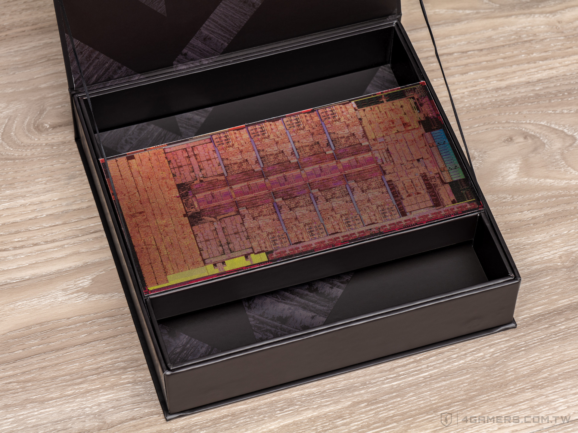
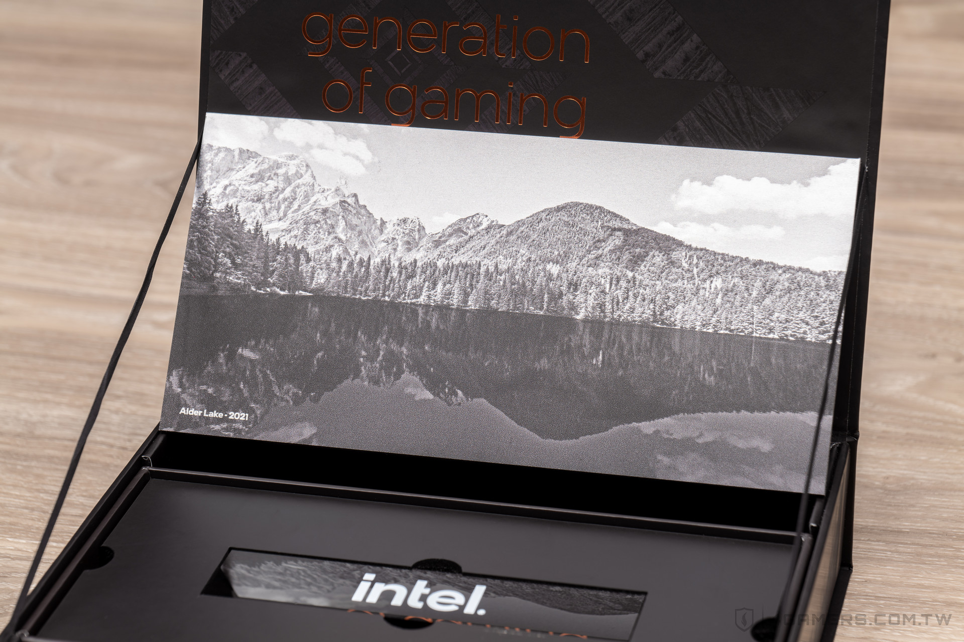
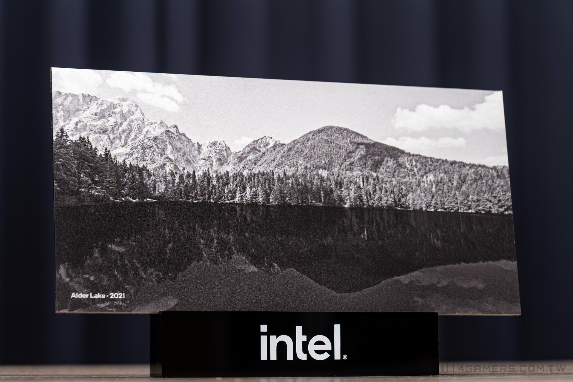
盒裝內特別附上一塊精心印製的 ;Alder Lake 晶圓照片,另一面則是位於美國華盛頓州 Alder Lake 的實景,確實別出心裁。
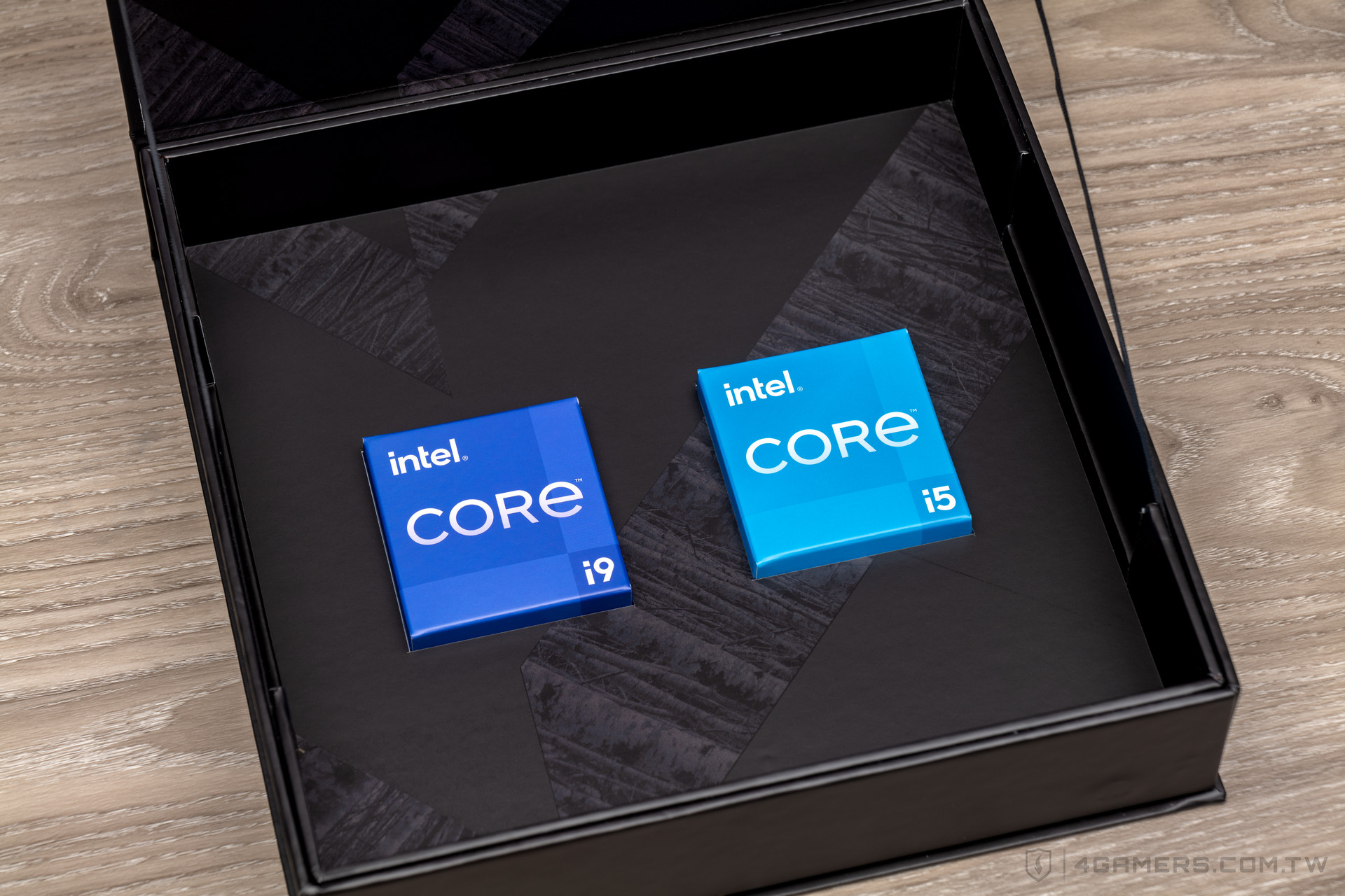
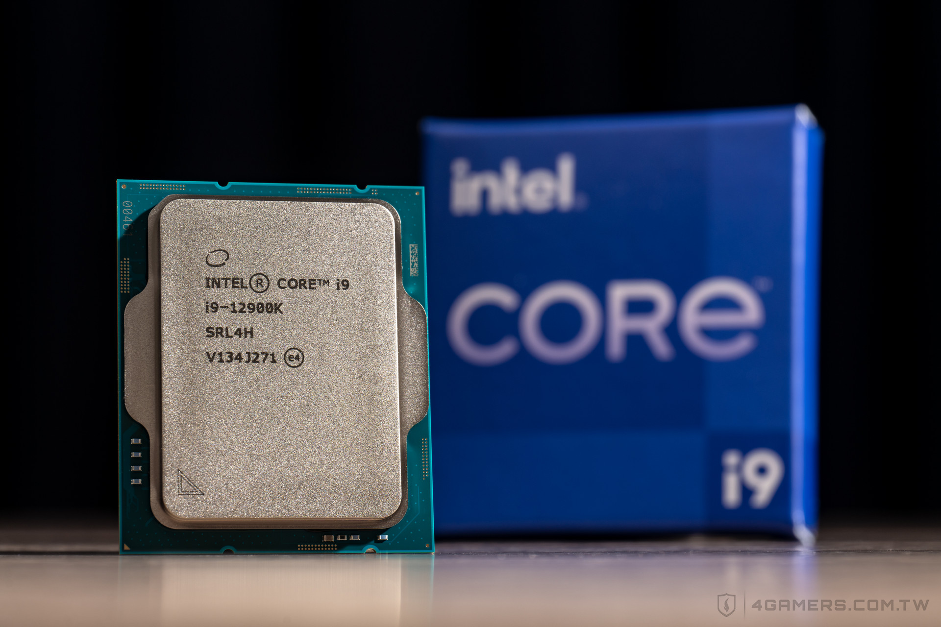
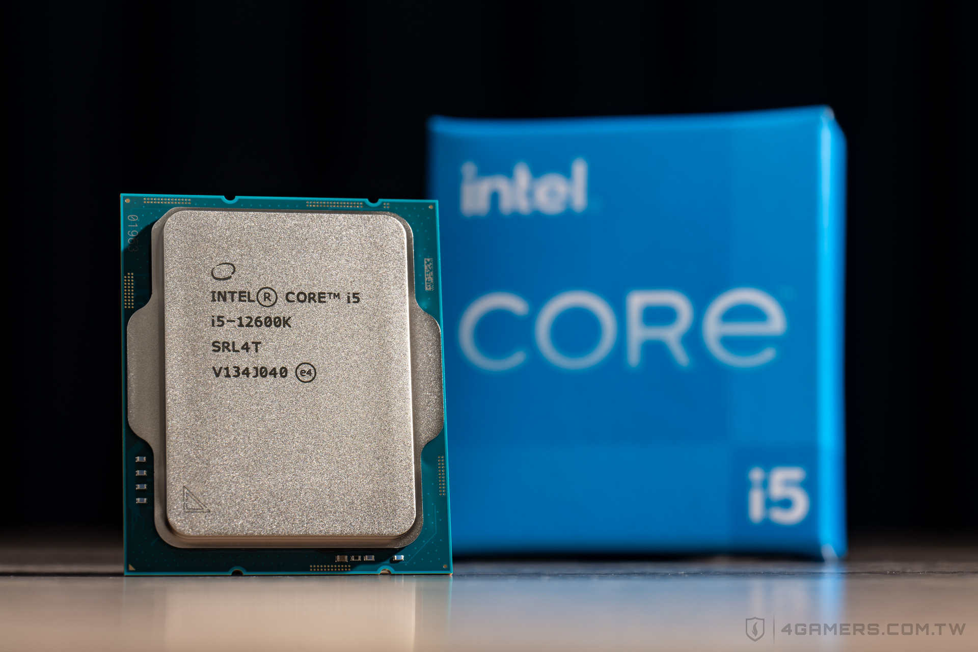
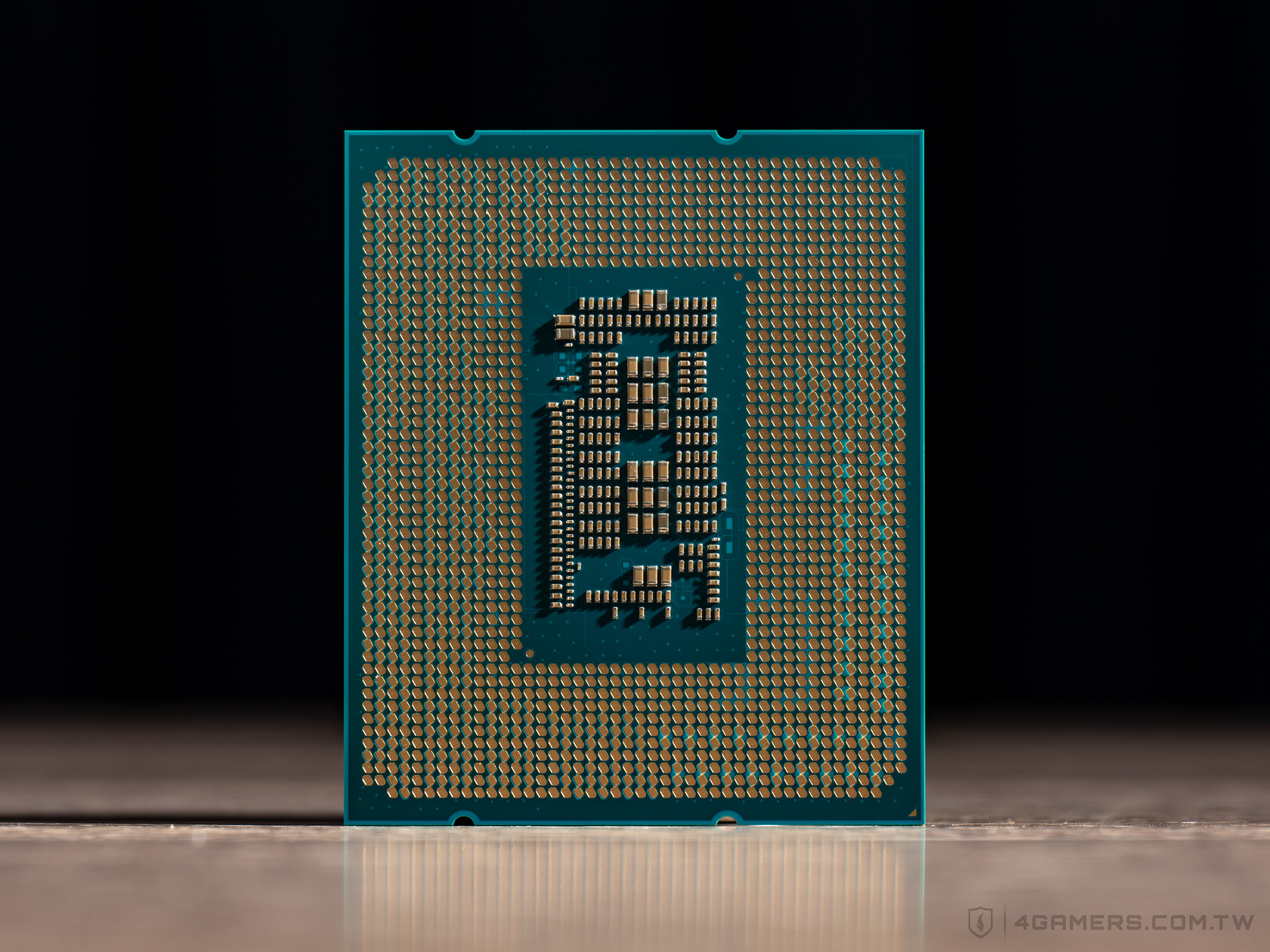
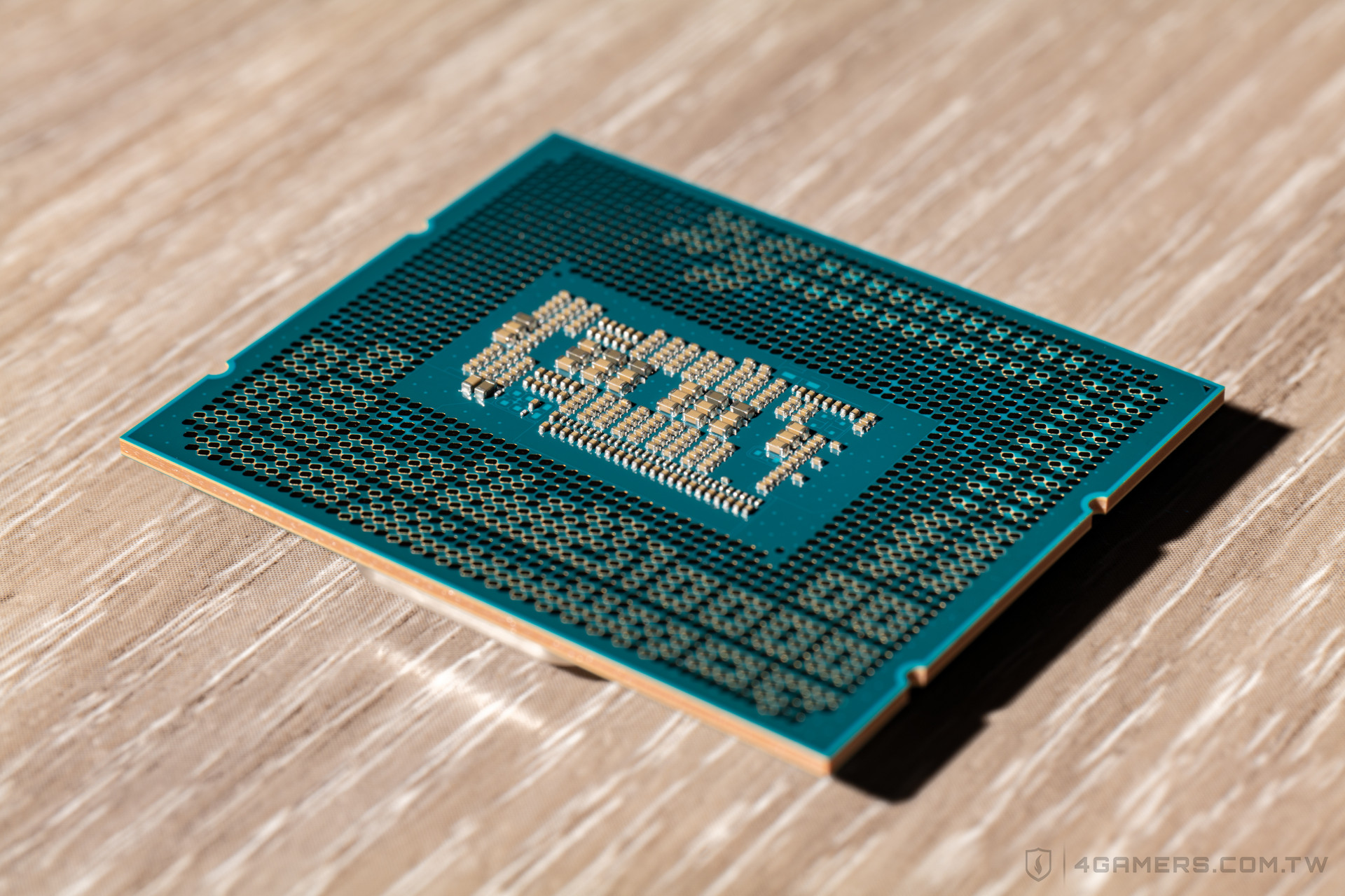
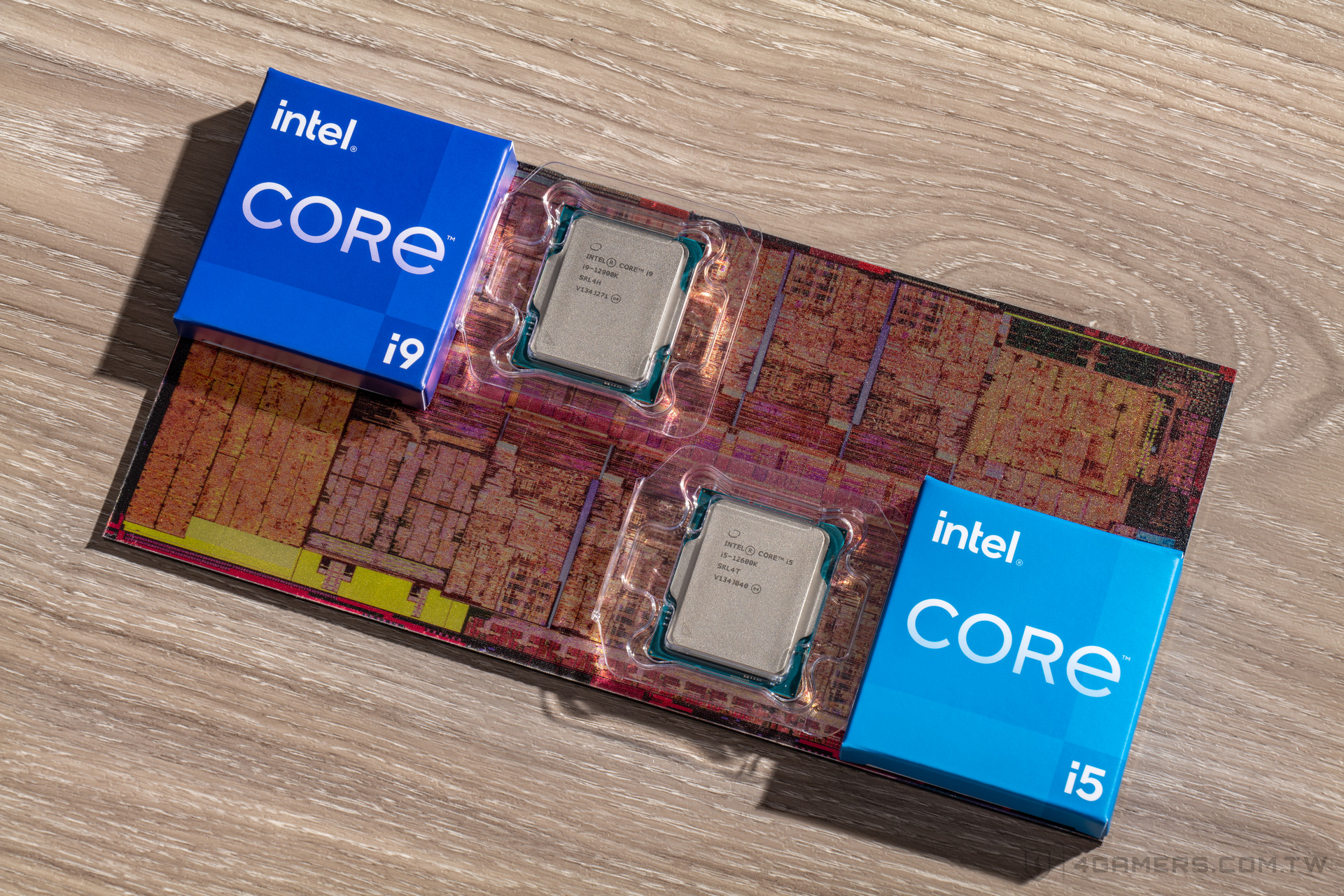
內含 Core i9-12900K 和 Core i5-12600K 處理器,皆為市售正式版。從外觀上已經可以很明顯看出第 12 代 Intel Core 處理器有別於以往,全新的 LGA 1700 封裝為 37.5 mm x 45 mm 長方形,因此散熱器扣具孔具也有所調整,詳細情形請靜待 11 月 4 日評測解禁。
Intel 近 10 年來最大幅度架構改進
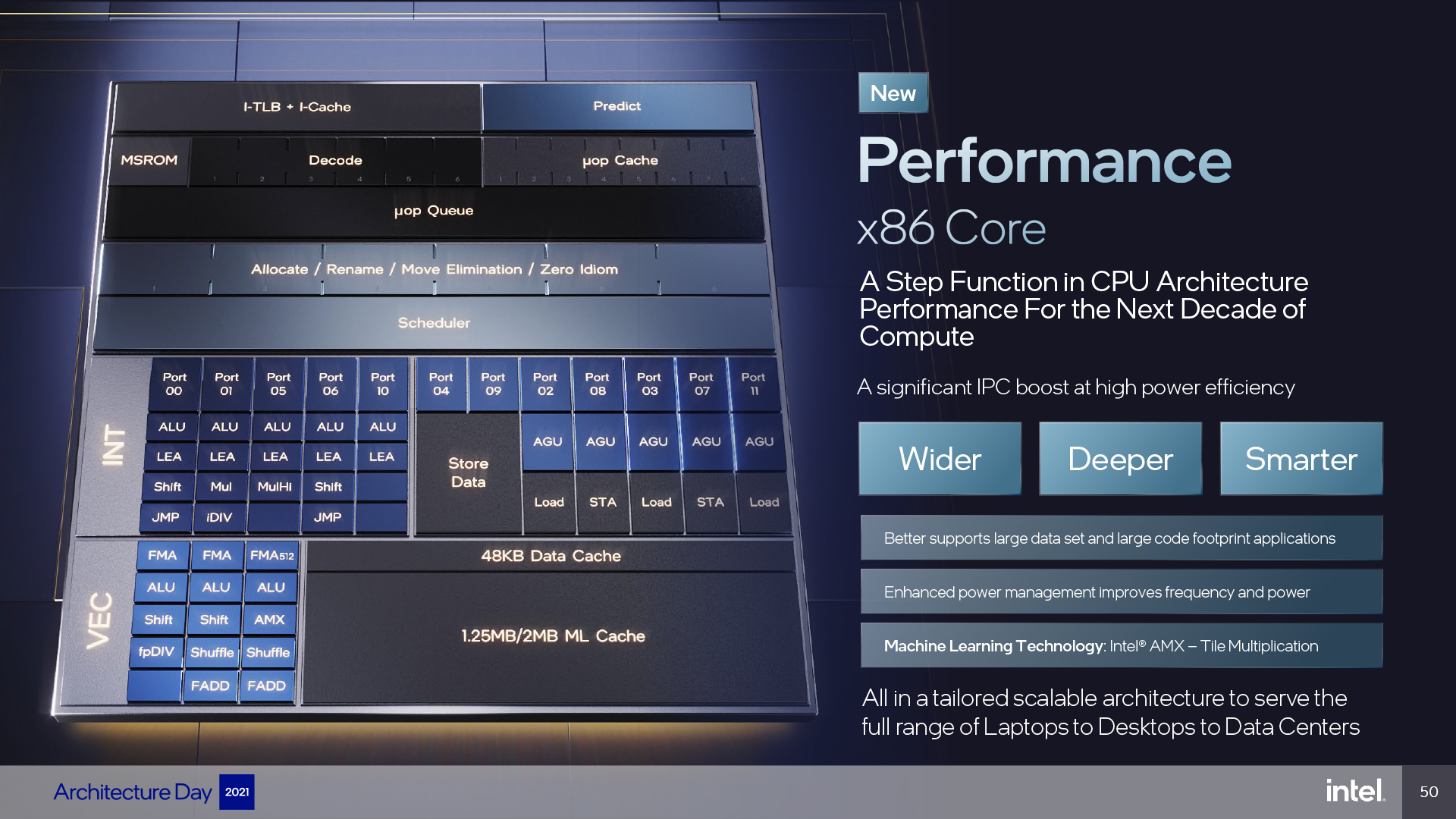
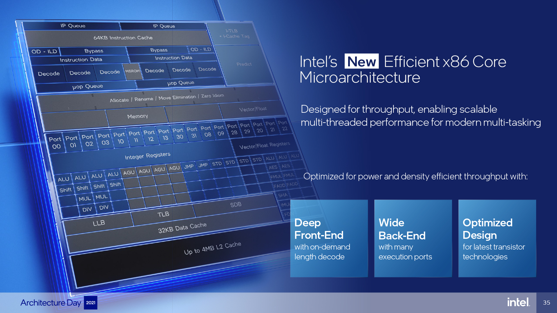
Alder Lake 處理器是 Intel 首度於主流效能級桌上型電腦導入的混合式核心架構,有別於過往的「大小核」稱呼,Intel 將其中兩種核心分別定名為 Performance Core (P-Core) 效能核心 與 Efficient Core (E-Core) 效率核心。
P-Core 效能核心微架構的先前代號為 Golden Cove,專為複雜且龐大的單執行緒運算提供低延遲且強大的效能,近似於現行各式桌上型處理器的核心。
E-Core 效率核心微架構的先前代號為 Gracemont,專門處理較不複雜但需要龐大吞吐量效率的運算,儘可能極小化晶圓面積,也允許核心在低電壓環境中運作降低功耗。
延伸閱讀:Intel Alder Lake 處理器 Gracemont 效率核心與 Goldencove 效能核心架構解析
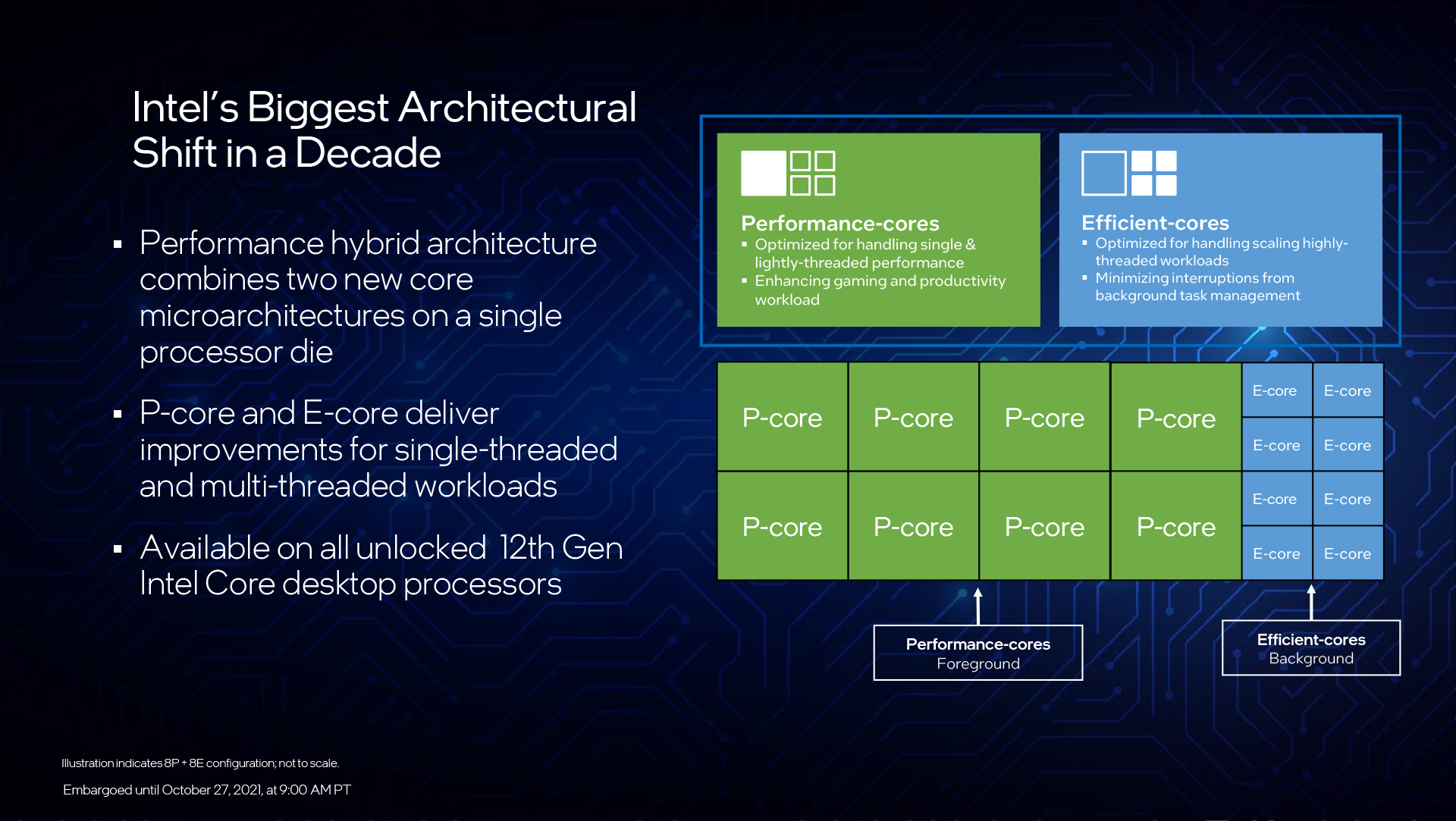
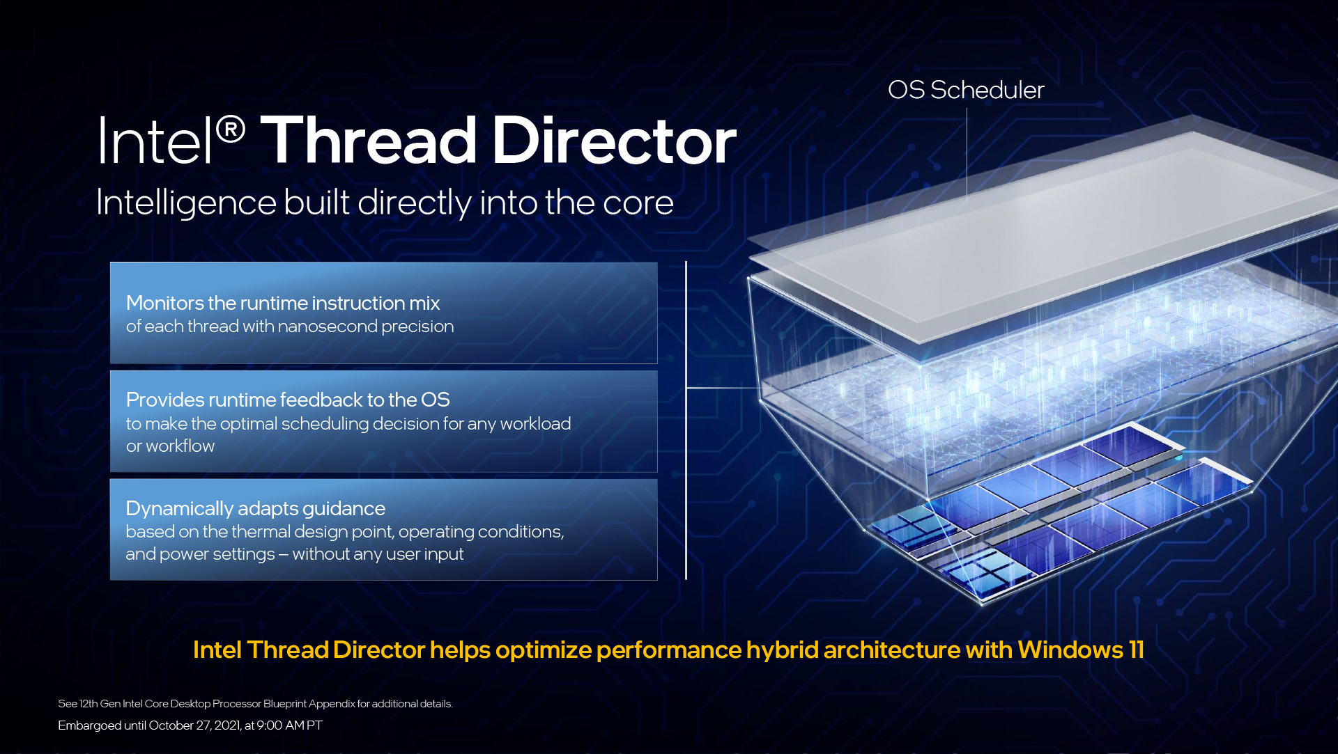
而為了要更妥善運用這兩種不同的核心架構,Intel 與微軟緊密合作,導入 Thread Director 技術。這是 Windows 11 才能啟用的專屬功能,能夠更精確分析程式負載屬性,並與作業系統排程器緊密溝通,動態調節核心資源給相對應的程式。
以最淺顯的方式說明,前景應用程式(通常包括遊戲與生產力軟體)由於直接面對使用者當前操作,會分配給延遲較低且時脈較高的 P-Core 效能核心進行處理。而背景應用程式相對來說不太需要即時反應,但還是需要相當程度的多緒執行,自然就分配給吞吐量大的 E-Core 效率核心了。
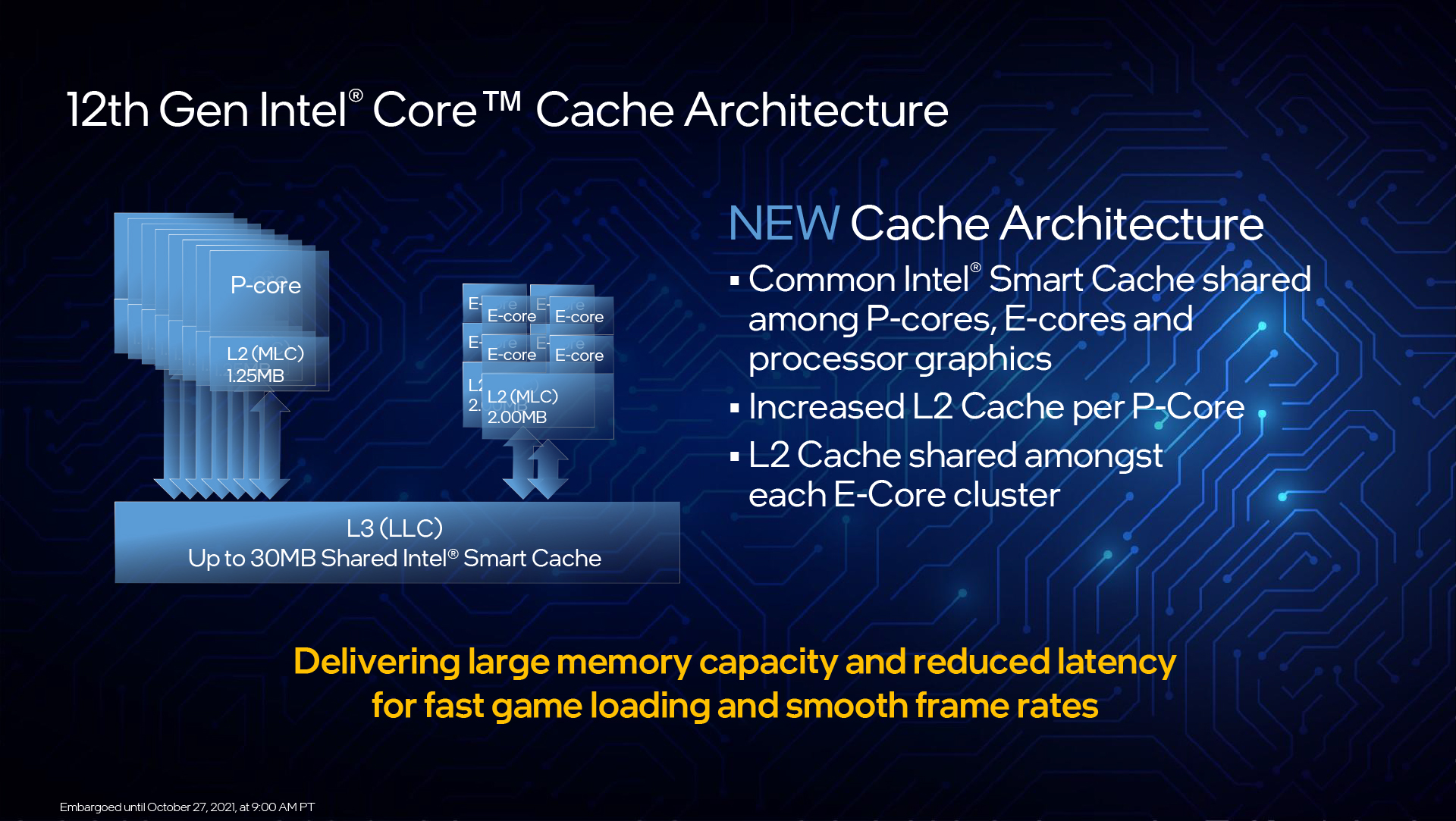
Alder Lake 處理器的快取記憶體也因應兩種不同核心導入新型態架構,每顆 P-Core 效能核心獨立擁有 1.25 MB 的 L2 快取 (MLC, Middle Level Cache),每組 E-Core 效率核心叢集(4 顆)共用 2 MB 的 L2 快取,而所有核心則共用最高 30 MB 的 L3 快取 (LLC, Last Level Cache)。
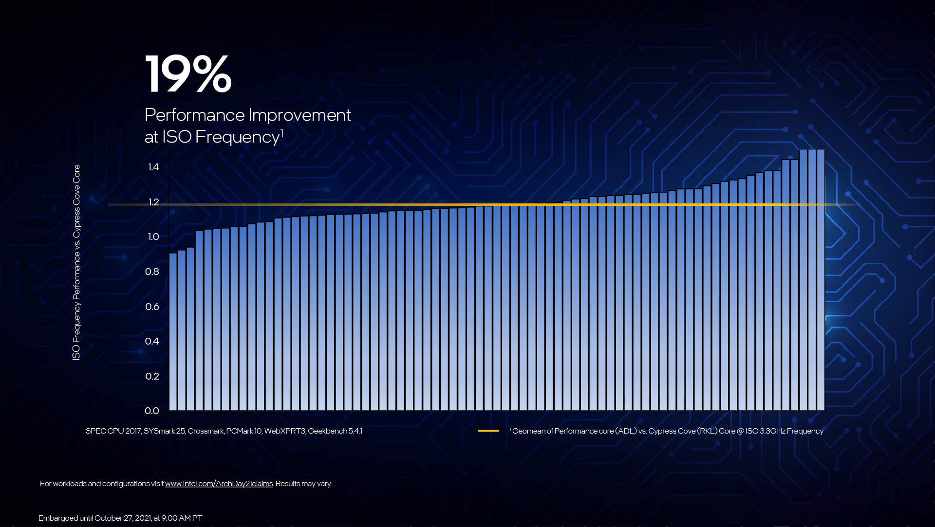
綜合以上所述,Alder Lake 處理器 P-Core 效能核心相較於前代 Rocket Lake 處理器的 Cypress Cove 核心,可提升約 19% 的 IPC(每時脈週期指令數量)效能。
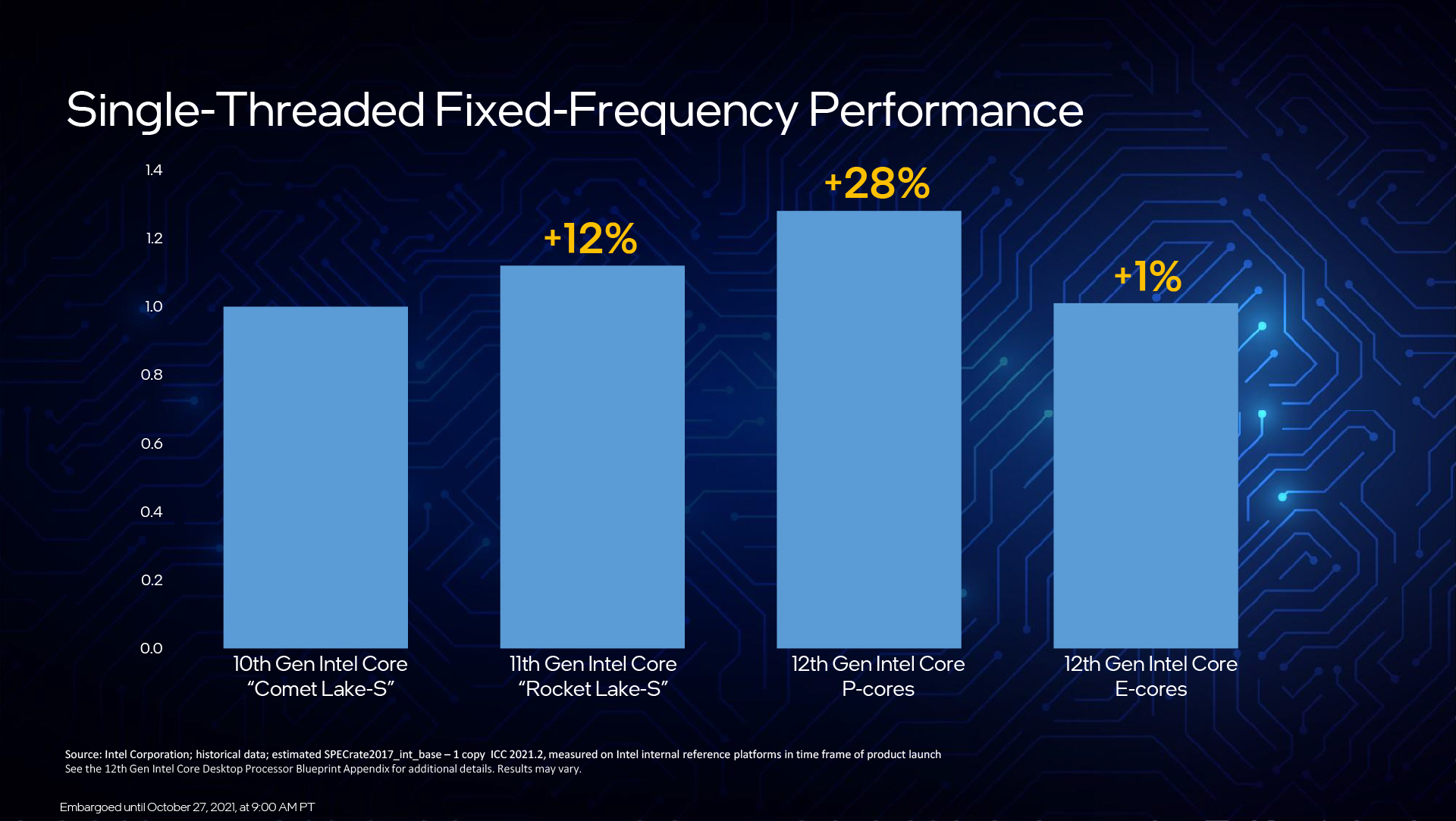
若在固定頻率單緒執行(單核)的情況下,以 Comet Lake-S 第 10 代 Core 處理器當作效能基準,Rocket Lake-S 第 11 代 Core 處理器提升了 12%,Alder Lake 第 12 代 Core 處理器的 P-Core 效能核心拓展至 28%,而 E-Core 效率核心則約莫相當於 Comet Lake-S 處理器(僅提升 1%)。
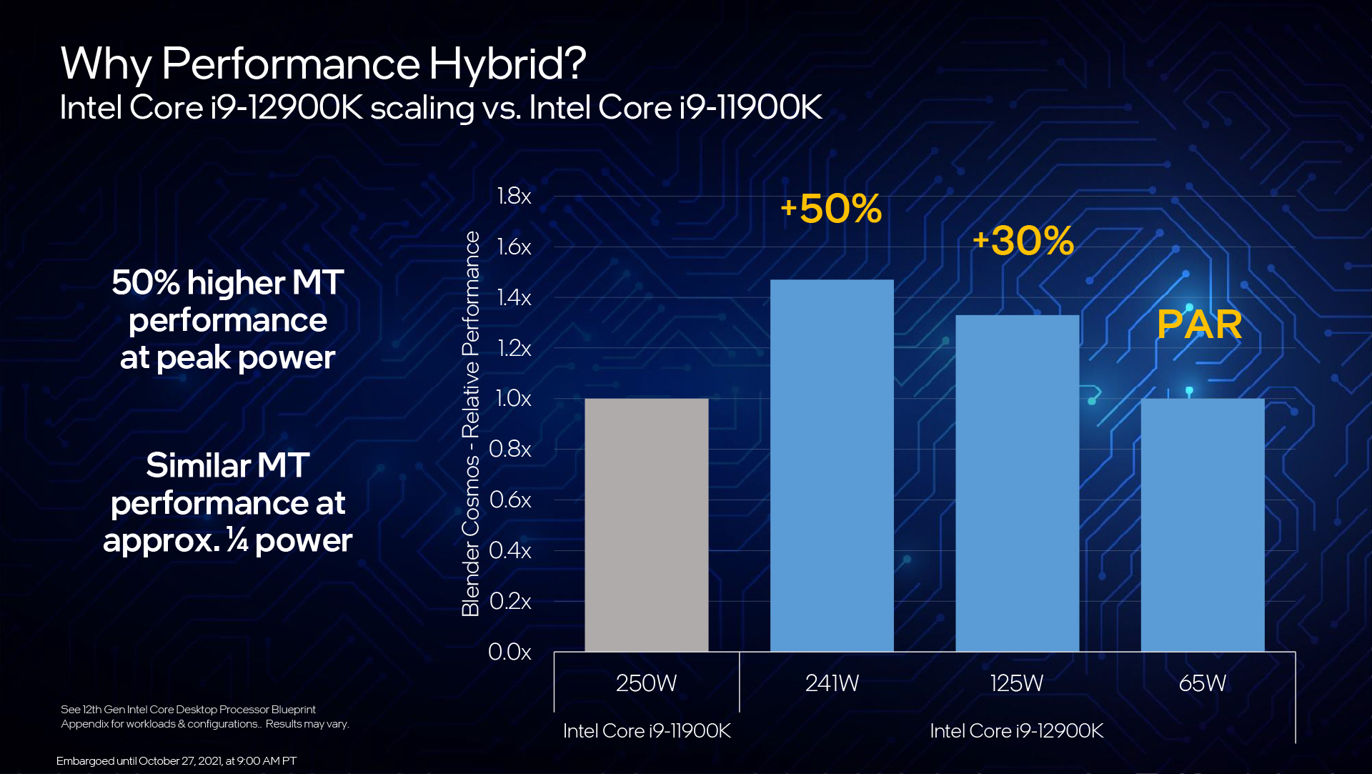
當然,功耗管理對於混和式核心架構更顯得重要。以 Core i9-11900K 的 PL2 250W 功耗當作基準,在相近的多核效能下,Core i9-12900K 只需要大約 65W,約 Core i9-11900K 的 4 分之 1;而在相近的尖峰功耗下,Core i9-12900K (PL2 241W) 可提供額外 50% 多核效能。
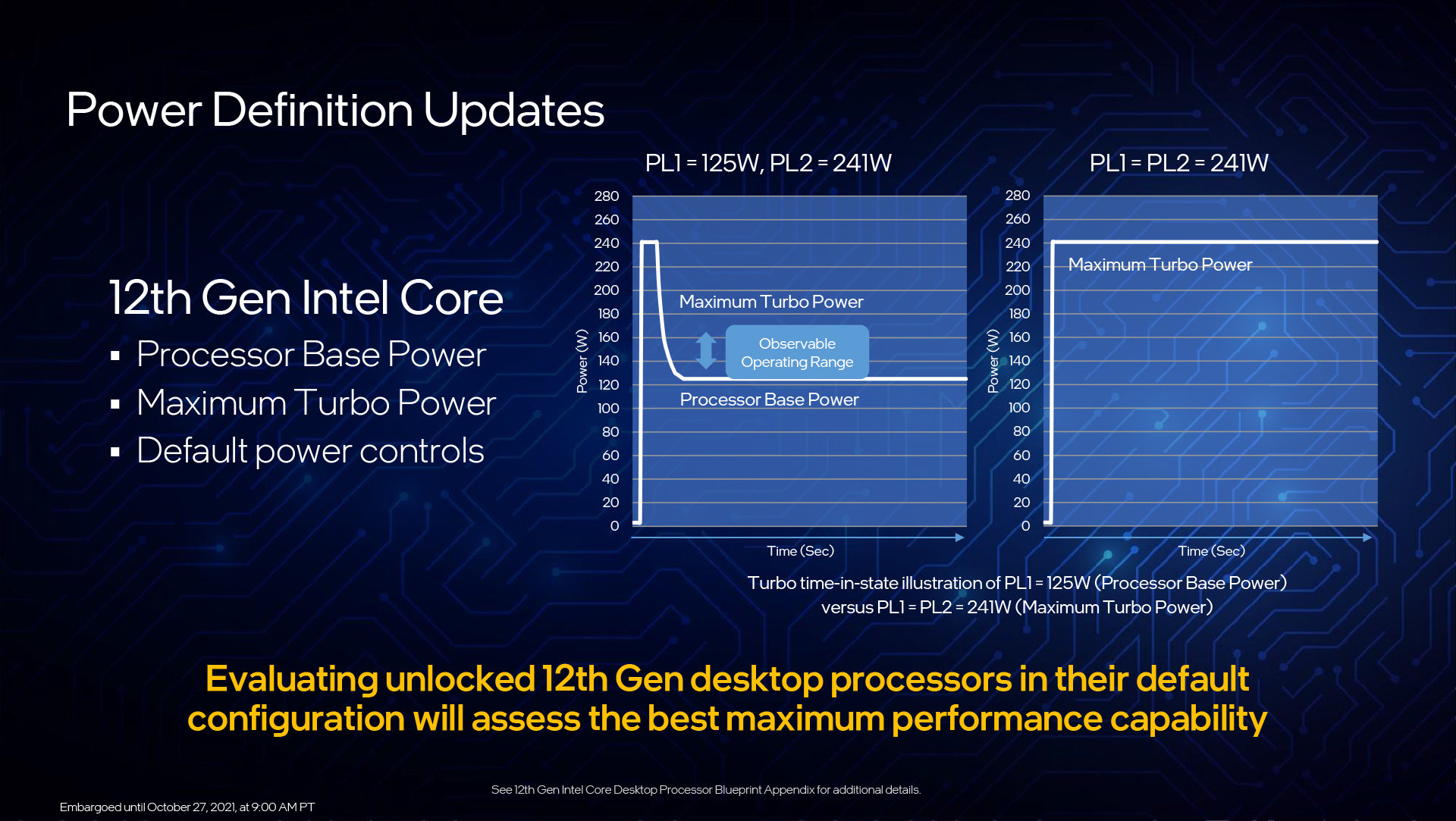
而相較過去時常造成混淆的 PL1 / PL2 TDP,Alder Lake 第 12 代 Core 處理器將其定名為「Processor Base Power(處理器基礎功耗)」與「Maximum Turbo Power(最大 Turbo 功耗)」。
第 12 代 Core 處理器在全預設狀態下,功耗大致維持在處理器基礎功耗,只有當需要特別重負載的時候才會推升到最大 Turbo 功耗。當然,使用者也可直接把處理器基礎功耗數值設定至最大 Turbo 功耗,這樣就能一直維持在最高效能狀態。
製程/封裝工藝再進化
第 12 代 Core 處理器總算捨棄沿用多年的 14nm 製程,這次使用的 Intel 7 製程原名 10nm SuperFin 強化版,是 Intel 當前最先進的量產製程技術,其表現近似於市面上其他 7nm 製程。
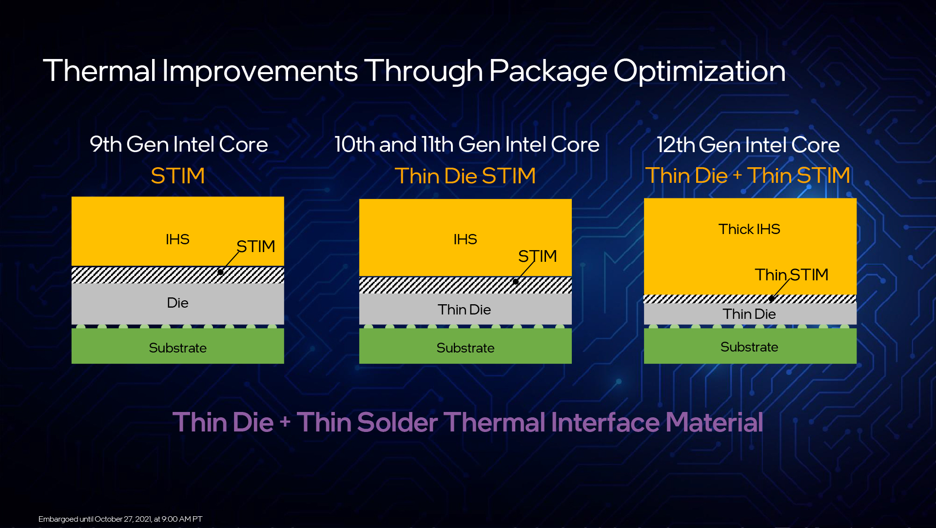
除了製程進一步微縮,晶圓封裝也有大幅改進。第 10 代、第 11 代 Core 處理器已做到薄型化晶圓(相較於第 9 代 Core 處理),而第 12 代 Core 處理器不只晶圓更薄,連導熱用的 STIM 焊接熱介面材料也打薄,取而代之的是使用較厚的 IHS 整合式散熱片,讓熱量更容易向外導出,不會堆積在晶圓內,有助於實現高時脈與超頻性。
傳輸頻寬再升級的 Z690 晶片組
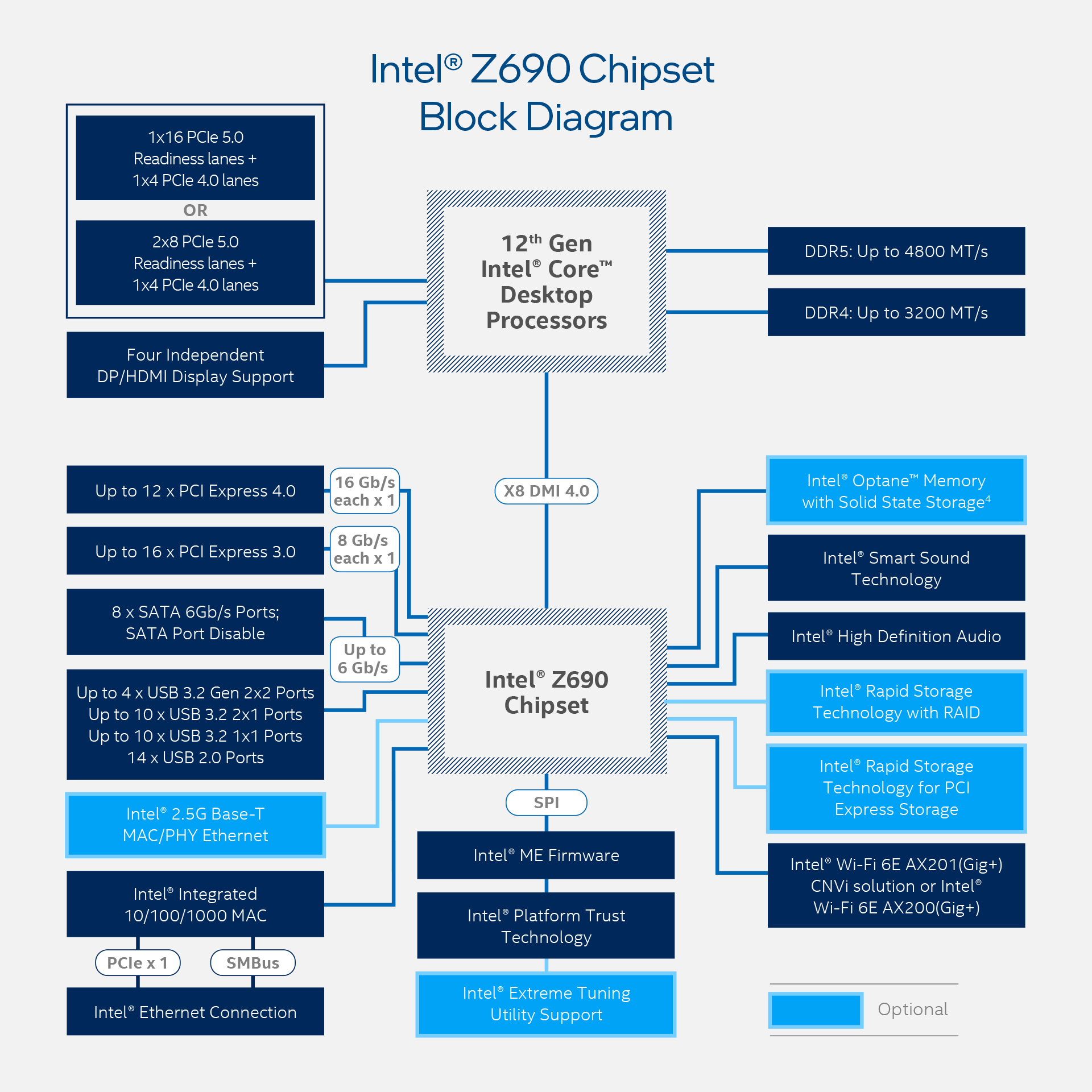
有別於 Z590 晶片組,Z690 才是真正導入 PCIe 4.0 介面的晶片組。它使用了 DMI 4.0 x8 介面與第 12 代 Core 處理器連通,頻寬相當於 PCIe 4.0 x8,是 Z590 晶片組的 2 倍。同時提供多達 12 條 PCIe 4.0 通道與 16 條 PCI 3.0 通道,使擴充性大幅提高。
較獨特的是,Z690 晶片組引進原本僅提供給伺服器晶片組的 Intel Volume Management Device (Intel VMD) 技術,讓 PCIe SSD 可串接成磁碟陣列。
更彈性的超頻架構
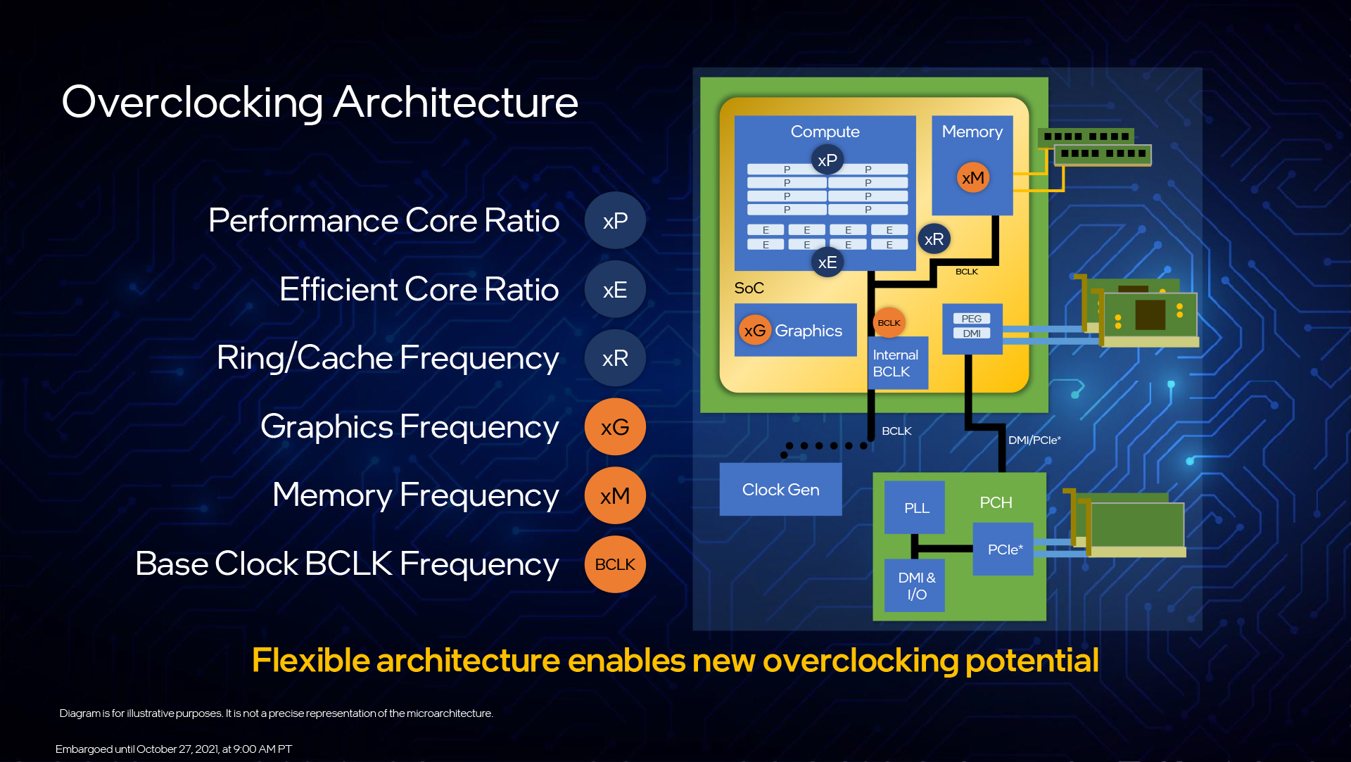
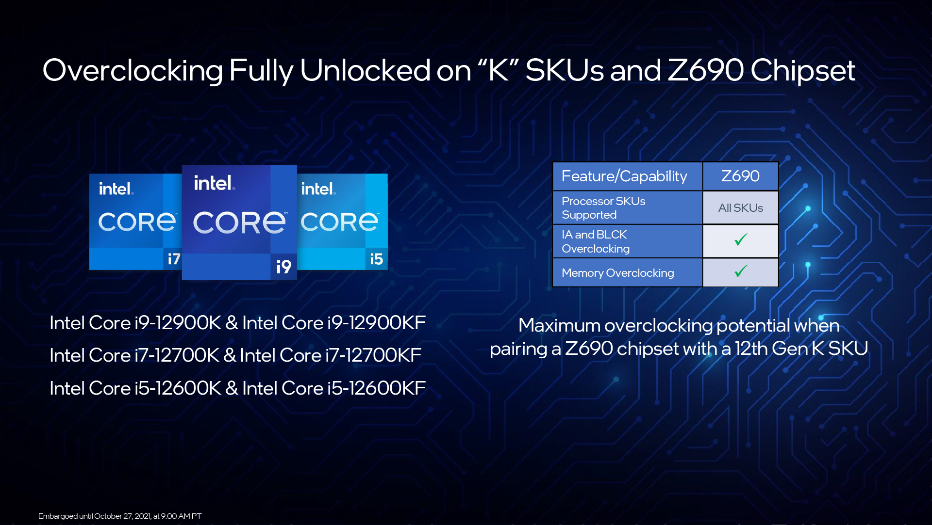
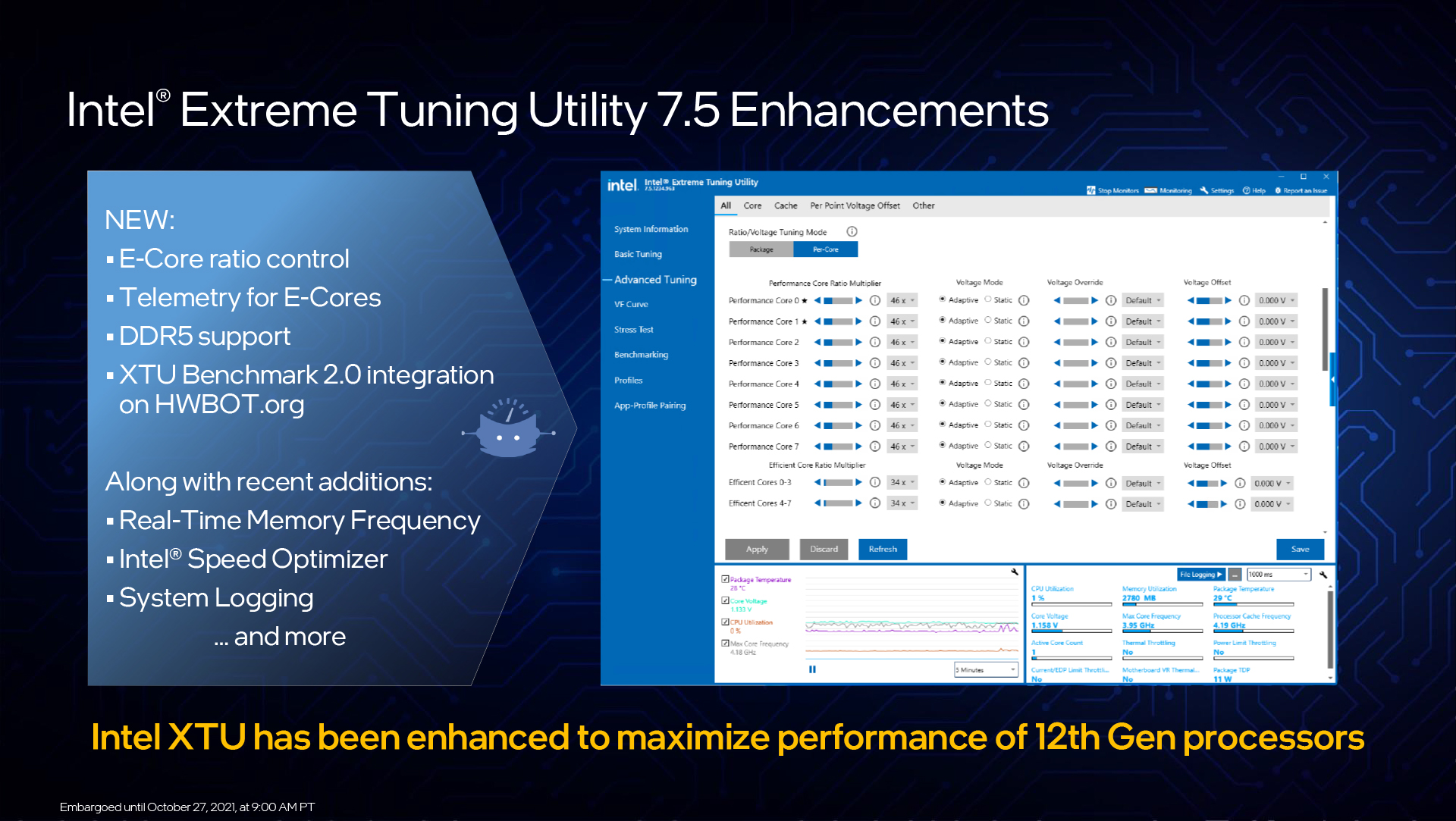
第 12 代 Core 處理器除了 K 系列提供的不鎖倍頻機制,可分別對 P-Core 效能核心 和 E-Core 效率核心設定不同的倍數進行超頻,快取記憶體倍頻也可獨立設定。這次還讓 BCLK(外頻)與 DMI / PCIe 通道脫鉤,可各自進行頻率調整。
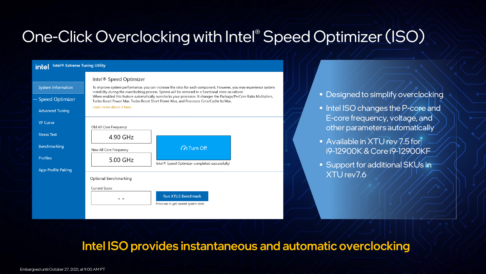
透過 Intel Extreme Tuning Utility 7.5 軟體,使用者可在作業系統內調整 E-Core 效率核心和 DDR5 記憶體超頻,也能運用 Intel Speed Optimizer (ISO) 一鍵完成簡易超頻。
導入 XMP 3.0 和 Dynamic Memory Boost 的 DDR5 記憶體
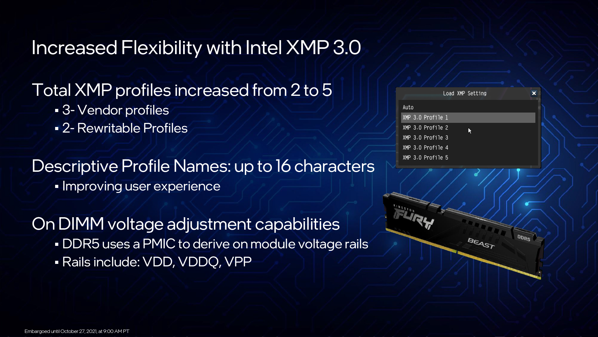
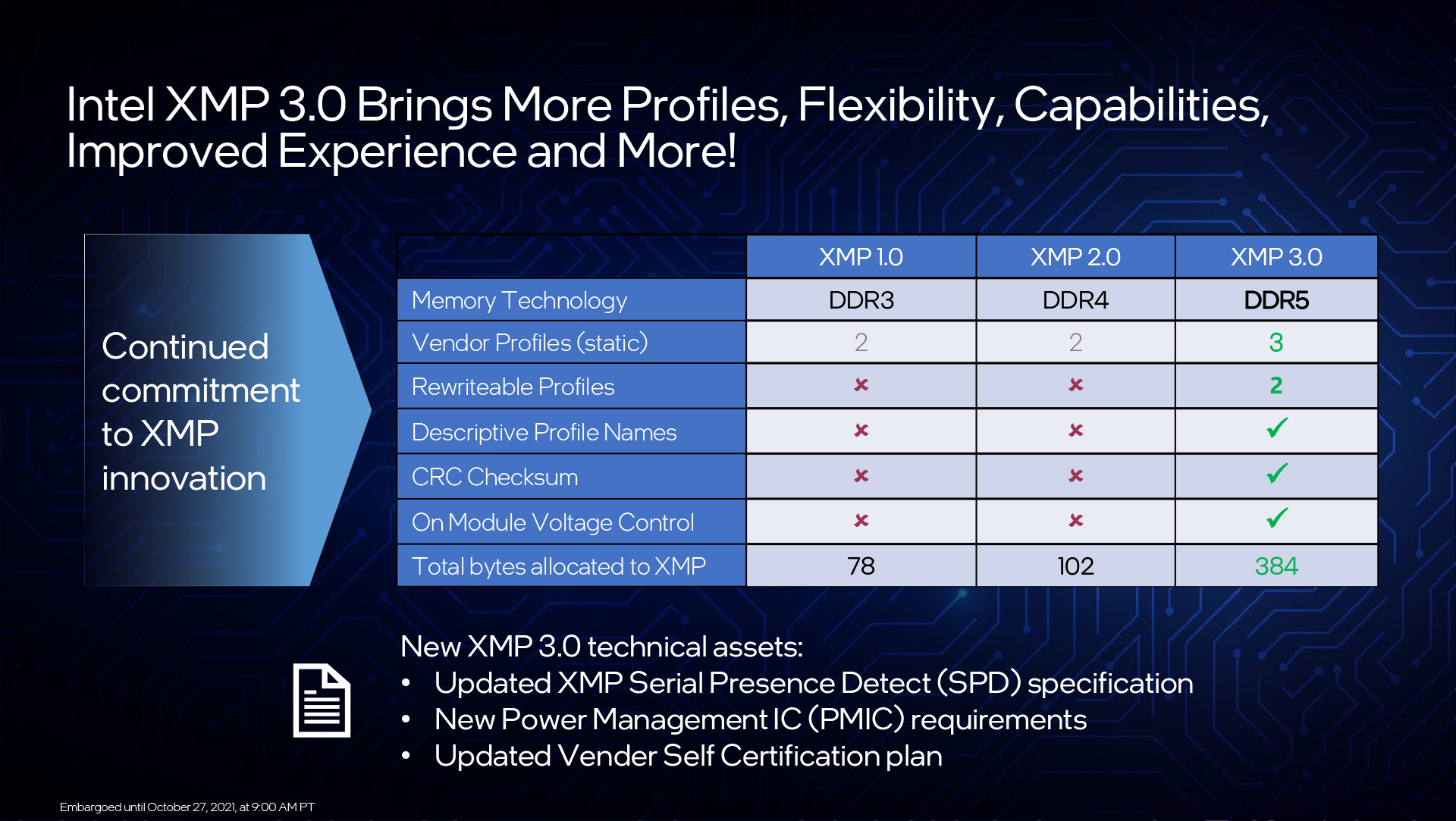
Intel 曾於 DDR3 / DDR4 記憶體分別導入 XMP 1.0 / XMP 2.0,這次 DDR5 記憶體除了更高的運作時脈,當然也導入 XMP 3.0 囉!
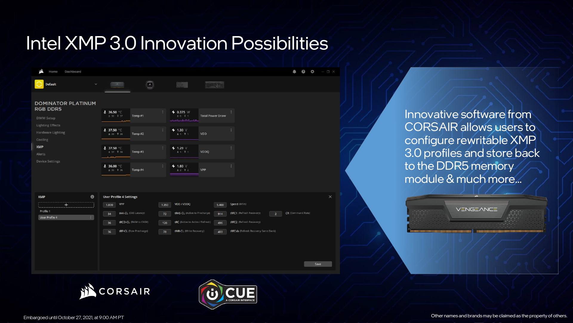
相較於 XMP 1.0 / XMP 2.0 只能由記憶體供應商設定且無法更改的 2 組 XMP 參數,XMP 3.0 不只開放 3 組供應商參數,還另外提供 2 組可重複寫入的自訂參數空間。像是 CORSAIR 的 iCUE 軟體就允許使用者自行調整記憶體參數並寫入 XMP 3.0。
而由於 DDR5 記憶體模組配有獨立的電源控制 IC(PMIC),因此可針對單一模組調整電壓,而非過去只能所有記憶體模組設定統一的電壓參數。
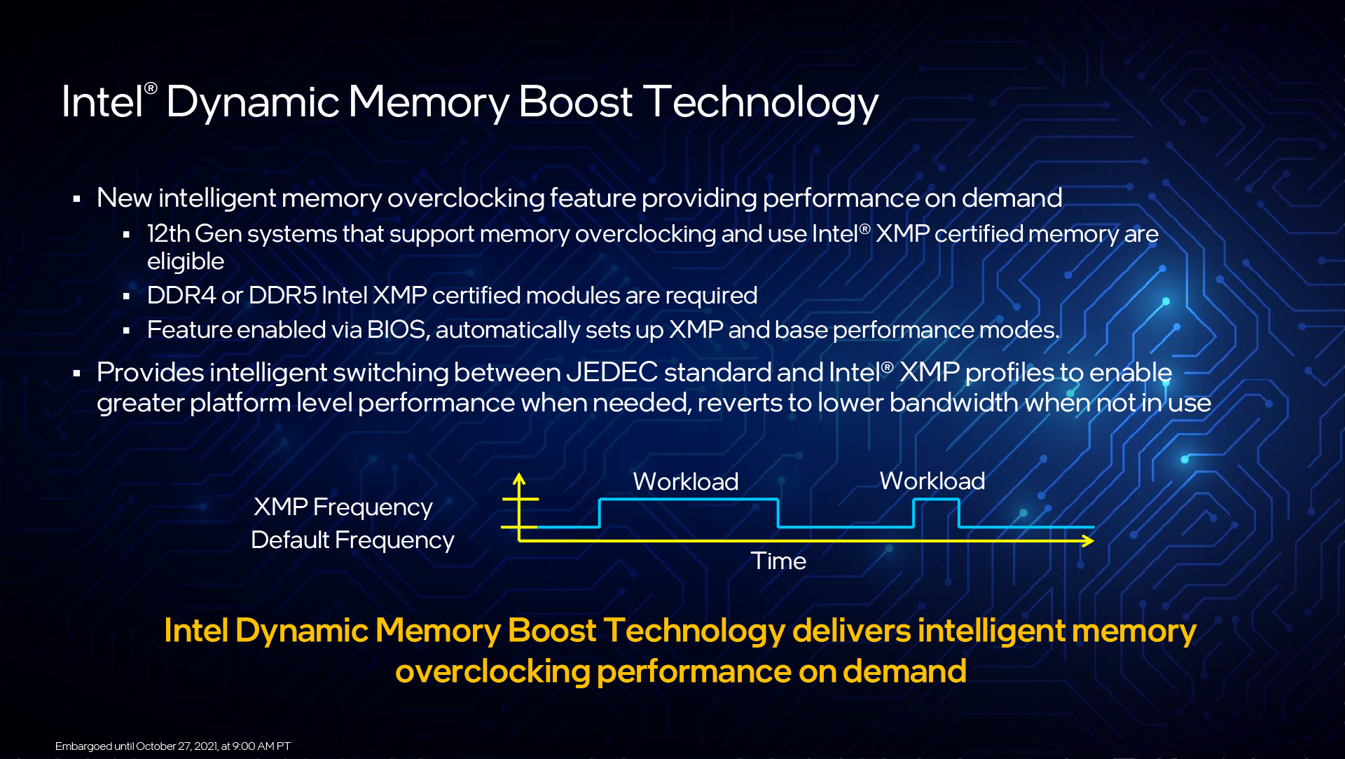
Dynamic Memory Boost 則是第 12 代 Core 處理器的新技術,可讓記憶體模組於一般閒置情況下以 JEDEC 標準時脈工作,而在工作負載需求加大的時候推升至 XMP 時脈。推估該功能是為筆記型電腦降低耗電而設計,桌上型電腦預設為關閉狀態。
靜待評測
更多效能測試與其他詳細資訊,請靜待台灣時間 11 月 4 日 21:00 解禁。
:quality(60):no_upscale()/https%3A%2F%2Fimg.4gamers.com.tw%2Fckfinder%2Ffiles%2FElvis%2FNews%2F2021-10%2FIntel%2FAlder-Lake%2F01.jpg)
:quality(60):no_upscale()/https%3A%2F%2Fimg.4gamers.com.tw%2Fckfinder%2Ffiles%2FElvis%2FNews%2F2021-10%2FIntel%2FAlder-Lake%2F03.jpg)
:quality(60):no_upscale()/https%3A%2F%2Fimg.4gamers.com.tw%2Fckfinder%2Ffiles%2FElvis%2FNews%2F2021-10%2FIntel%2FAlder-Lake%2F02.jpg)
:quality(60):no_upscale()/https%3A%2F%2Fimg.4gamers.com.tw%2Fckfinder%2Ffiles%2FElvis%2FNews%2F2021-10%2FIntel%2FAlder-Lake%2F33.jpg)
:quality(60):no_upscale()/https%3A%2F%2Fimg.4gamers.com.tw%2Fckfinder%2Ffiles%2FElvis%2FNews%2F2021-10%2FIntel%2FAlder-Lake%2F04.jpg)
:quality(60):no_upscale()/https%3A%2F%2Fimg.4gamers.com.tw%2Fckfinder%2Ffiles%2FElvis%2FNews%2F2021-10%2FIntel%2FAlder-Lake%2F05.jpg)
:quality(60):no_upscale()/https%3A%2F%2Fimg.4gamers.com.tw%2Fckfinder%2Ffiles%2FElvis%2FReview%2FIntel-Core-i9-12900K-and-i5-12600K%2F01.jpg)
:quality(60):no_upscale()/https%3A%2F%2Fimg.4gamers.com.tw%2Fckfinder%2Ffiles%2FElvis%2FReview%2FIntel-Core-i9-12900K-and-i5-12600K%2F07.jpg)
:quality(60):no_upscale()/https%3A%2F%2Fimg.4gamers.com.tw%2Fckfinder%2Ffiles%2FElvis%2FReview%2FIntel-Core-i9-12900K-and-i5-12600K%2F09.jpg)
:quality(60):no_upscale()/https%3A%2F%2Fimg.4gamers.com.tw%2Fckfinder%2Ffiles%2FElvis%2FReview%2FIntel-Core-i9-12900K-and-i5-12600K%2F10.jpg)
:quality(60):no_upscale()/https%3A%2F%2Fimg.4gamers.com.tw%2Fckfinder%2Ffiles%2FElvis%2FReview%2FIntel-Core-i9-12900K-and-i5-12600K%2F11.jpg)
:quality(60):no_upscale()/https%3A%2F%2Fimg.4gamers.com.tw%2Fckfinder%2Ffiles%2FElvis%2FReview%2FIntel-Core-i9-12900K-and-i5-12600K%2F12.jpg)
:quality(60):no_upscale()/https%3A%2F%2Fimg.4gamers.com.tw%2Fckfinder%2Ffiles%2FElvis%2FReview%2FIntel-Core-i9-12900K-and-i5-12600K%2F13.jpg)
:quality(60):no_upscale()/https%3A%2F%2Fimg.4gamers.com.tw%2Fckfinder%2Ffiles%2FElvis%2FReview%2FIntel-Core-i9-12900K-and-i5-12600K%2F14.jpg)
:quality(60):no_upscale()/https%3A%2F%2Fimg.4gamers.com.tw%2Fckfinder%2Ffiles%2FElvis%2FReview%2FIntel-Core-i9-12900K-and-i5-12600K%2F18.jpg)
:quality(60):no_upscale()/https%3A%2F%2Fimg.4gamers.com.tw%2Fckfinder%2Ffiles%2FElvis%2FReview%2FIntel-Core-i9-12900K-and-i5-12600K%2F19.jpg)
:quality(60):no_upscale()/https%3A%2F%2Fimg.4gamers.com.tw%2Fckfinder%2Ffiles%2FElvis%2FReview%2FIntel-Core-i9-12900K-and-i5-12600K%2F24.jpg)
:quality(60):no_upscale()/https%3A%2F%2Fimg.4gamers.com.tw%2Fckfinder%2Ffiles%2FElvis%2FReview%2FIntel-Core-i9-12900K-and-i5-12600K%2F25.jpg)
:quality(60):no_upscale()/https%3A%2F%2Fimg.4gamers.com.tw%2Fckfinder%2Ffiles%2FElvis%2FNews%2F2021-10%2FIntel%2FAlder-Lake%2F06.jpg)
:quality(60):no_upscale()/https%3A%2F%2Fimg.4gamers.com.tw%2Fckfinder%2Ffiles%2FElvis%2FNews%2F2021-08%2FIntel%2Fintel-architecture-day-2021-presentation-50.jpg)
:quality(60):no_upscale()/https%3A%2F%2Fimg.4gamers.com.tw%2Fckfinder%2Ffiles%2FElvis%2FNews%2F2021-08%2FIntel%2Fintel-architecture-day-2021-presentation-35.jpg)
:quality(60):no_upscale()/https%3A%2F%2Fimg.4gamers.com.tw%2Fckfinder%2Ffiles%2FElvis%2FNews%2F2021-10%2FIntel%2FAlder-Lake%2F07.jpg)
:quality(60):no_upscale()/https%3A%2F%2Fimg.4gamers.com.tw%2Fckfinder%2Ffiles%2FElvis%2FNews%2F2021-10%2FIntel%2FAlder-Lake%2F08.jpg)
:quality(60):no_upscale()/https%3A%2F%2Fimg.4gamers.com.tw%2Fckfinder%2Ffiles%2FElvis%2FNews%2F2021-10%2FIntel%2FAlder-Lake%2F09.jpg)
:quality(60):no_upscale()/https%3A%2F%2Fimg.4gamers.com.tw%2Fckfinder%2Ffiles%2FElvis%2FNews%2F2021-10%2FIntel%2FAlder-Lake%2F10.jpg)
:quality(60):no_upscale()/https%3A%2F%2Fimg.4gamers.com.tw%2Fckfinder%2Ffiles%2FElvis%2FNews%2F2021-10%2FIntel%2FAlder-Lake%2F11.jpg)
:quality(60):no_upscale()/https%3A%2F%2Fimg.4gamers.com.tw%2Fckfinder%2Ffiles%2FElvis%2FNews%2F2021-10%2FIntel%2FAlder-Lake%2F12.jpg)
:quality(60):no_upscale()/https%3A%2F%2Fimg.4gamers.com.tw%2Fckfinder%2Ffiles%2FElvis%2FNews%2F2021-10%2FIntel%2FAlder-Lake%2F13.jpg)
:quality(60):no_upscale()/https%3A%2F%2Fimg.4gamers.com.tw%2Fckfinder%2Ffiles%2FElvis%2FNews%2F2021-10%2FIntel%2FAlder-Lake%2F14.jpg)
:quality(60):no_upscale()/https%3A%2F%2Fimg.4gamers.com.tw%2Fckfinder%2Ffiles%2FElvis%2FNews%2F2021-10%2FIntel%2FAlder-Lake%2F15.png)
:quality(60):no_upscale()/https%3A%2F%2Fimg.4gamers.com.tw%2Fckfinder%2Ffiles%2FElvis%2FNews%2F2021-10%2FIntel%2FAlder-Lake%2F16.jpg)
:quality(60):no_upscale()/https%3A%2F%2Fimg.4gamers.com.tw%2Fckfinder%2Ffiles%2FElvis%2FNews%2F2021-10%2FIntel%2FAlder-Lake%2F17.jpg)
:quality(60):no_upscale()/https%3A%2F%2Fimg.4gamers.com.tw%2Fckfinder%2Ffiles%2FElvis%2FNews%2F2021-10%2FIntel%2FAlder-Lake%2F18.jpg)
:quality(60):no_upscale()/https%3A%2F%2Fimg.4gamers.com.tw%2Fckfinder%2Ffiles%2FElvis%2FNews%2F2021-10%2FIntel%2FAlder-Lake%2F19.jpg)
:quality(60):no_upscale()/https%3A%2F%2Fimg.4gamers.com.tw%2Fckfinder%2Ffiles%2FElvis%2FNews%2F2021-10%2FIntel%2FAlder-Lake%2F20.jpg)
:quality(60):no_upscale()/https%3A%2F%2Fimg.4gamers.com.tw%2Fckfinder%2Ffiles%2FElvis%2FNews%2F2021-10%2FIntel%2FAlder-Lake%2F21.jpg)
:quality(60):no_upscale()/https%3A%2F%2Fimg.4gamers.com.tw%2Fckfinder%2Ffiles%2FElvis%2FNews%2F2021-10%2FIntel%2FAlder-Lake%2F22.jpg)
:quality(60):no_upscale()/https%3A%2F%2Fimg.4gamers.com.tw%2Fckfinder%2Ffiles%2FElvis%2FNews%2F2021-10%2FIntel%2FAlder-Lake%2F23.jpg)
:quality(60):no_upscale()/https%3A%2F%2Fimg.4gamers.com.tw%2Fckfinder%2Ffiles%2FElvis%2FReview%2FIntel-Core-i9-12900K-and-i5-12600K%2F16.jpg)